

Integrated high-speed all-optical wavelength conversion device
An all-optical wavelength conversion and integrated device technology, applied in the field of optoelectronics, can solve the problems of difficult integration, inability to achieve integration, and large volume of the wavelength conversion device, so as to overcome the large volume, overcome the electron rate bottleneck, improve throughput and The effect of transparency
- Summary
- Abstract
- Description
- Claims
- Application Information
AI Technical Summary
Problems solved by technology
Method used
Image

Examples
Embodiment Construction
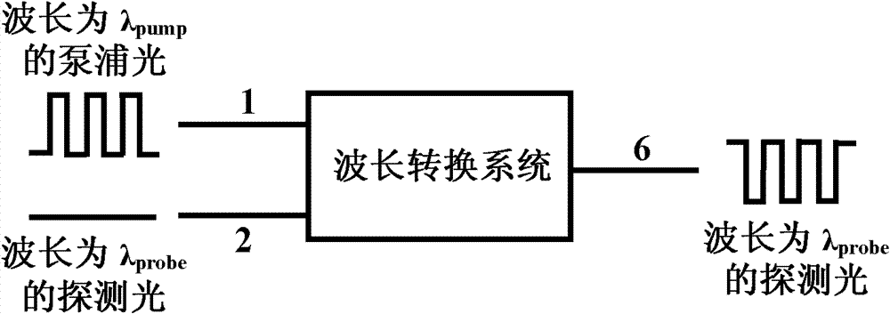
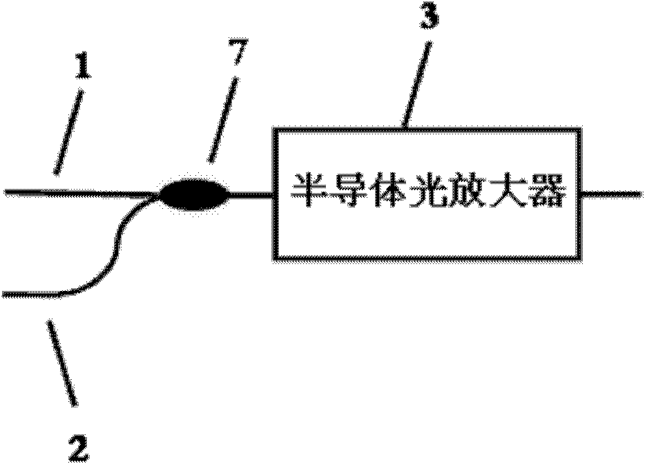
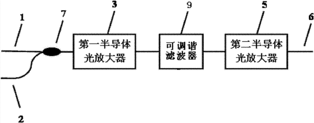
[0024] An integrated device for high-speed all-optical wavelength conversion, such as Figure 4 As shown, it includes an optical power coupler 7, a first semiconductor optical amplifier 3, an electroabsorption modulator 4 and a second semiconductor optical amplifier 5; the wavelength is λ pump The pulsed light carrying the digital signal is input from an input terminal 1 of the optical power coupler 7 as pump light, and the wavelength is λ probe The continuous light is input from another input end 2 of the optical power coupler 7 as the probe light, and the pump light and the probe light are coupled into the first semiconductor optical amplifier 3 after being coupled by the optical power coupler 7; the first semiconductor optical amplifier 3 converts the wavelength for lambda pump The digital signal carried by the pump light is modulated to a wavelength of λ probe On the probe light, the wavelength conversion is realized; the pump light and probe light output from the first ...
PUM
 Abstract
Description
Claims
Application Information