
Alkali metal doping treatment method for large-scale production of copper indium gallium selenide thin film solar cells

A solar cell, copper indium gallium selenide technology, applied in circuits, electrical components, photovoltaic power generation and other directions, can solve the problems of complex process flow, generation of hydrogen selenide, long return time, etc., to reduce the deposition thickness and the overall cadmium content. , the effect of improving performance

Active Publication Date: 2021-06-04
ZHEJIANG SHANGYUE OPTOELECTRONICS TECH +1
View PDF4 Cites 0 Cited by
  • Summary
  • Abstract
  • Description
  • Claims
  • Application Information

AI Technical Summary

Problems solved by technology

[0010] (3) Alkali metal doping after the deposition of CIGS absorption layer on flexible substrates requires two processes, and requires a long return time, and the complex and time-consuming process is not conducive to large-scale production
[0011] Since some alkali metal materials are easy to absorb water during the addition process, this will cause some hydrogen selenide to be generated during the doping process of alkali metals. After opening the cavity, if excessive hydrogen selenide is inhaled, it will easily cause poisoning symptoms and cause safety problems.

Method used


Image

  • Alkali metal doping treatment method for large-scale production of copper indium gallium selenide thin film solar cells
  • Alkali metal doping treatment method for large-scale production of copper indium gallium selenide thin film solar cells
  • Alkali metal doping treatment method for large-scale production of copper indium gallium selenide thin film solar cells

Examples


Embodiment 1

[0058] A base metal doping treatment method when the copper indium gallium-producing film solar cell is largely produced, and the steps are as follows:

[0059] 1. A DC magnetron sputtering method is deposited on the substrate on the substrate on the substrate at a thickness of 25 μm flexible thin film substrate (stainless steel), deposits a layer of 0.4 μm thick Mo back electrode layer.

[0060] 2. Add 1700 g of silica gel desiccant as a water absorbing agent in the reaction device, in a vacuum is 1 × 10 -3 The substrate was heated to 150 ° C in the co-evaporation chamber of the PA, and a layer of NaF layer was evaporated on the surface of the Mo back electrode layer, and the NAF evaporation source temperature was 760-800 ° C, and the evaporation time was 10 min.

[0061] 3. The substrate temperature is increased to 480 ° C, circulate in, Ga, SE, where the in the evaporation source temperature is from 940 to 1050 ° C, the Ga evaporation source temperature is from 1050 to 1200 ° C...

Embodiment 2

[0072] A base metal doping treatment method when the copper indium gallium-producing film solar cell is largely produced, and the steps are as follows:

[0073] 1. A DC magnetron sputtering method is deposited on the substrate on the substrate in a thickness of 40 μm flexible thin film substrate (polyimide), deposits a layer of 0.8 μm thick Mo back electrode layer.

[0074] 2. Add 1800 g of anhydrocalized calcium chloride as a water absorbing agent in the reaction apparatus, at a vacuum is 3 × 10 -3 The substrate was heated to 300 ° C in the conjunction of the PA, and a layer of Naf layer was evaporated on the surface of the Mo back electrode layer, and the NAF evaporation source temperature was 760-800 ° C, and the evaporation time was 20 min.

[0075] 3. The substrate temperature is increased to 600 ° C, circulate in, Ga, SE, where the in evaporation source temperature is from 940 to 1050 ° C, Ga evaporation source temperature is 1050-1200 ° C, SE evaporation source temperature ...

Embodiment 3

[0086] A base metal doping treatment method when the copper indium gallium-producing film solar cell is largely produced, and the steps are as follows:

[0087] 1. A DC magnetron sputtering method is deposited on the substrate on the substrate at a thickness of 30 μm flexible film substrate (stainless steel) to deposit a layer of 0.6 μm thick Mo back electrode layer.

[0088] 2. Add 2000 g of silica gel desiccant as a water absorbing agent in the reaction device, 2 × 10 in vacuo -3 The substrate is heated to 200 ° C in the conjunction of the PA, and a layer of NaF layer is evaporated, and the NaF evaporation source temperature is 760-800 ° C, the evaporation time is 15 min.

[0089] 3. The substrate temperature is increased to 550 ° C, circulate in, Ga, SE, where the in the evaporation source temperature is from 940 to 1050 ° C, the Ga evaporation source temperature is from 1050 to 1200 ° C, the SE evaporation source temperature is 450-500 ° C, The evaporation time was 15 min.

[00...


PUM

PropertyMeasurementUnit
thicknessaaaaaaaaaa
thicknessaaaaaaaaaa
thicknessaaaaaaaaaa

Abstract

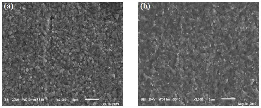
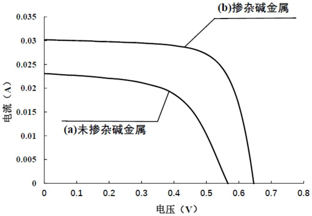
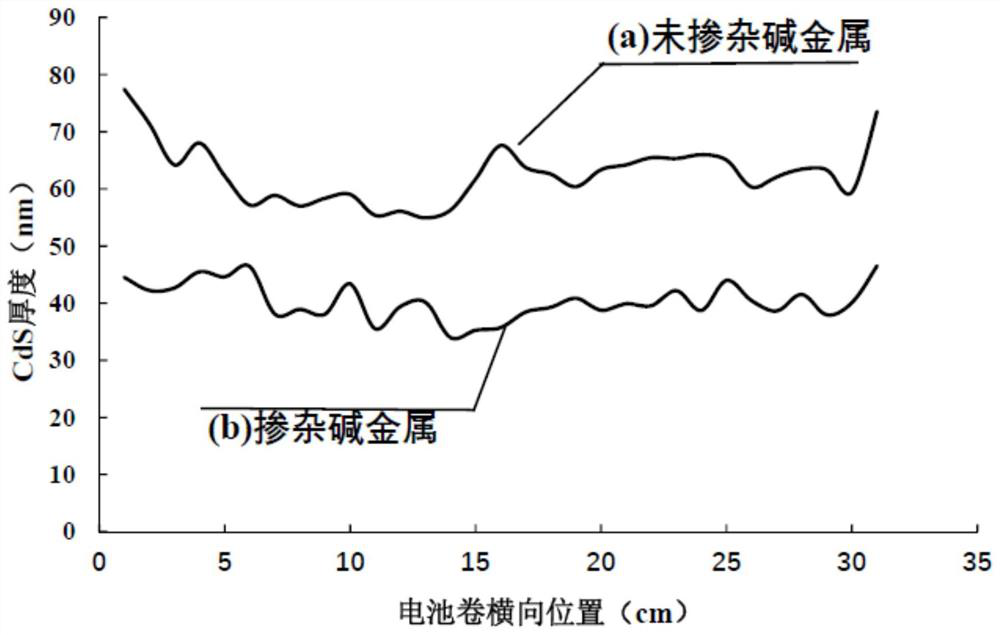
The invention discloses an alkali metal doping treatment method for large-scale production of copper indium gallium selenide thin film solar cells, which comprises the following steps in sequence: (1) first depositing a layer of Mo back electrode layer; (2) depositing a layer of alkali Metal halide; (3) co-evaporate In, Ga, and the sixth main group solid element again, (4) re-co-evaporate Cu, the sixth main group solid element; (5) deposit another layer of alkali metal halide; (6 ) Co-evaporating Cu and the sixth main group solid element; (7) Co-evaporating In, Ga, and the sixth main group solid element; (8) finally depositing a layer of alkali metal halide; (9) annealing treatment. The invention can effectively increase the adhesion between the Mo layer and the CIGS layer, increase the CIGS hole concentration, reduce the surface roughness of the film, reduce the thickness of the CdS buffer layer, and improve the open circuit voltage and photoelectric conversion efficiency of the thin film solar cell.

Description

Technical field [0001] The present invention relates to the field of production techniques of thin film photovoltaic devices, and more particularly to an alkali metal doping treatment method when a copper indium gallium selenium film solar cell is mass-produced. Background technique [0002] Solar energy as clean energy has developed rapidly, and the installed capacity of solar cells is increasing at nearly 25% per year. By 2017, the global cumulative installed capacity has exceeded 402.5GW, showing a good momentum. According to IT IT (IEA), by 2030, it is expected to reach 1721GW, and by 2050 will rise to 4670GW, and the development potential of the photovoltaic industry is huge. [0003] The high-efficiency thin film solar cell is collectively referred to as a copper indium gallium selenium (CIGS battery), and the CIGS film solar cell is a solar cell. It is characterized by high technical requirements, carryable, no light. The phenomenon of causing activity, high conversion eff...

Claims


Application Information

Patent Timeline
Patent Type & Authority Patents(China)
IPC IPC(8): H01L31/18
CPCH01L31/18H01L31/186H01L31/1864Y02E10/50Y02P70/50
Inventor 胡煜霖刘宽菲任宇航
Owner ZHEJIANG SHANGYUE OPTOELECTRONICS TECH
Learn More