Semiconductor package and manufacturing method

A manufacturing method and packaging technology, which are applied to semiconductor devices, semiconductor/solid-state device components, electric solid-state devices, etc., can solve the problems of obvious reflow process, affecting packaging reliability, and reducing process yield.

Pending Publication Date: 2020-06-05
CHANGXIN MEMORY TECH INC
View PDF0 Cites 1 Cited by
  • Summary
  • Abstract
  • Description
  • Claims
  • Application Information

AI Technical Summary

Problems solved by technology

However, when a larger size interposer substrate is used as a support element for a semiconductor package, it often has significant warpage, especially during the reflow proc...

Method used


Image

  • Semiconductor package and manufacturing method
  • Semiconductor package and manufacturing method
  • Semiconductor package and manufacturing method

Examples


Embodiment 1

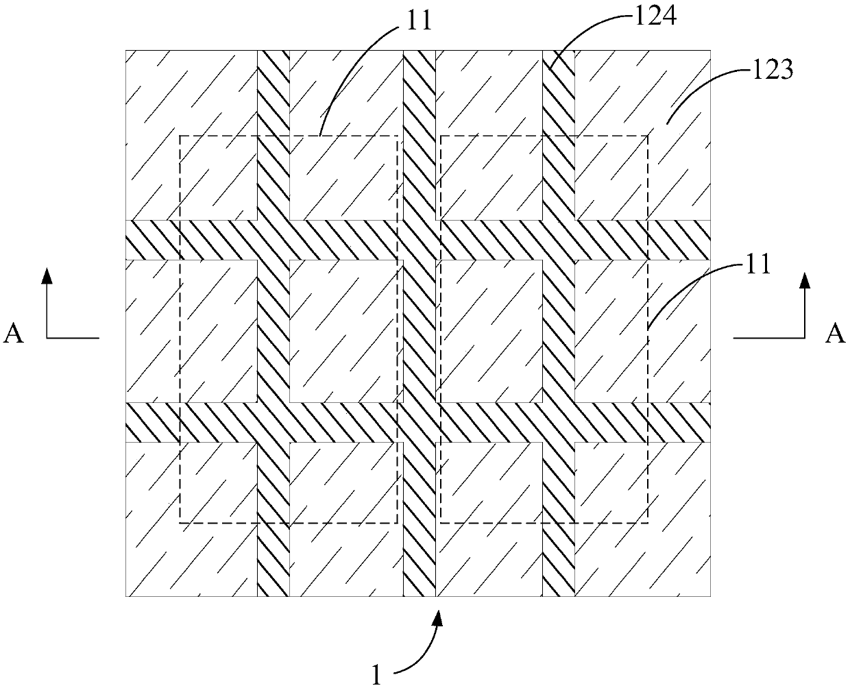
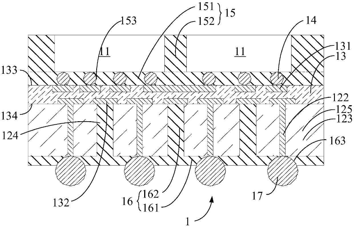
[0062] figure 1 , 2 The structure of a semiconductor package 1 in this embodiment is shown. The semiconductor package 1 includes a plurality of interposers 123 , a plurality of chips 11 , a plurality of first connectors 14 , a plurality of second connectors 17 and a redistribution layer 13 . A plurality of first connecting elements 14 and a plurality of intermediary elements 123 are respectively fixed on two sides of the redistribution layer 13 . Multiple chips 11 are fixed on the first connector 14 . The second connecting element 17 is disposed on a side of the interposer 123 away from the redistribution layer 13 . The two chips 11 can be electrically connected to each other through the redistribution layer 13 , and the chips 11 are electrically connected to the second connection member 17 through the first connection member 14 , the redistribution layer 13 , and the intermediary member 123 connected in sequence. The second connector 17 can be used as a pin of the semicon...

Embodiment 2

[0109] The semiconductor package 1a in the second embodiment differs from the semiconductor package 1 in the first embodiment only in the interposer and the groove. For the sake of brevity, only the structure and shape of the intermediary member 123a and the groove 124a in the second embodiment will be described below.

[0110] refer to Figure 12 , In this embodiment, the intermediary member 123a is a right triangle. The intermediaries 123a are provided in pairs. The hypotenuses of the two intermediary pieces 123a arranged in pairs are parallel to each other and close to each other, and the groove 124a separates the hypotenuses of the two intermediary pieces 123a. There are two pairs of intermediary members 123a, and the two pairs of intermediary members 123a are separated from each other by grooves 124a. Two chips 11a are provided, and each chip 11a can be projected onto a pair of interposers 123a arranged in pairs.

[0111] Since a groove 124a is formed between two adja...

Embodiment 3

[0113] The semiconductor package 1b in the third embodiment differs from the semiconductor package 1 in the first embodiment only in the interposer and the groove. For the sake of brevity, only the intermediary member 123b and the groove 124b in the third embodiment are described below.

[0114] refer to Figure 13 , in this embodiment, the intermediary member 123b is rectangular. The intermediary 123b is provided with four pieces. Two adjacent intermediary pieces 123b are separated from each other, and a groove 124b is formed between two adjacent intermediary pieces 123b. The grooves 124 are connected to form a "cross" structure. There are two chips 11b, one chip 11b can be projected onto two intermediary pieces 123b, and the other chip 11b can be projected onto the other two intermediary pieces 123b.

[0115] Since a groove 124b is formed between two adjacent interposers 123b, the groove 124b is an expansion joint of the intermediary substrate composed of a plurality of ...


PUM


Abstract

The invention discloses a semiconductor package and a manufacturing method. The semiconductor package comprises a rewiring layer, a plurality of first connecting pieces, a plurality of chips, a plurality of intermediate pieces and a plurality of second connecting pieces, wherein the rewiring layer comprises a first surface and a second surface opposite to the first surface; the plurality of firstconnecting pieces are connected to the first surface of the rewiring layer; the plurality of chips are all arranged on one side, deviating from the rewiring layer, of the first connecting pieces and are all connected to the first connecting pieces; the plurality of intermediate pieces are connected to the second surface of the rewiring layer, a groove is formed between every two adjacent intermediate pieces, and one side surface, close to the rewiring layer, of each groove is in direct contact with the second surface of the rewiring layer; and the plurality of second connecting pieces are connected to one side, deviating from the rewiring layer, of the intermediate pieces, and the chip is electrically connected to the second connecting pieces through the first connecting pieces, the rewiring layer and the intermediate pieces. The arrangement of the groove can effectively prevent the semiconductor package from cracking due to warping of an intermediate substrate in the manufacturing process, and the yield of the semiconductor package is improved.

Description

technical field [0001] The present invention generally relates to a semiconductor device packaging technology, and specifically relates to a semiconductor package and a manufacturing method. Background technique [0002] With the rapid development of wireless communication, automotive electronics and other consumer electronics, microelectronic packaging technology is developing in the direction of multi-function, miniaturization, portability, high speed, low power consumption and high reliability. In order to realize the miniaturization, high speed and modularization of electronic devices, one of the packaging technologies is to package multiple chips together to form a packaged device, and then mount the packaged device on a printed circuit board. [0003] In the existing multi-chip packaging technology, multiple chips are usually packaged on an intermediary substrate. As the number of chips increases or the size of the chip increases, the size of the intermediary substrate...

Claims


Application Information

Patent Timeline
IPC IPC(8): H01L23/498H01L23/48H01L23/31H01L25/07
CPCH01L23/3128H01L23/481H01L23/49816H01L23/49838H01L25/072H01L2224/16225H01L2924/15311H01L2924/181H01L2924/18161H01L2924/00012
Inventor 不公告发明人
Owner CHANGXIN MEMORY TECH INC
Why Eureka
Try Eureka