Semiconductor laser and manufacturing method thereof

A manufacturing method and a technology of lasers, which are applied to semiconductor lasers, lasers, laser parts, etc., can solve problems such as high prices, unfavorable mass production of devices, and difficult processing and production

Active Publication Date: 2021-04-23
INST OF SEMICONDUCTORS - CHINESE ACAD OF SCI
View PDF10 Cites 0 Cited by
  • Summary
  • Abstract
  • Description
  • Claims
  • Application Information

AI Technical Summary

Problems solved by technology

However, the tip width of the speckle converter is very small, in the range of 0.5-1 micron, which is difficult to manufacture using traditional contact photolithography.
Fine microstructures can be obtained using the electron beam exposure process, but this equipment is expensive and takes a long time to process, which is not conducive to mass production of devices

Method used


Image

  • Semiconductor laser and manufacturing method thereof
  • Semiconductor laser and manufacturing method thereof
  • Semiconductor laser and manufacturing method thereof

Examples


Embodiment Construction

[0021] In order to make the object, technical solution and advantages of the present invention clearer, the present invention will be further described in detail below in conjunction with specific embodiments and with reference to the accompanying drawings.

[0022] The invention discloses a semiconductor laser and a manufacturing method thereof. The mold speckle converter integrated on the semiconductor laser can be realized by a common contact photolithography process, which is beneficial to reducing the manufacturing cost of the device.

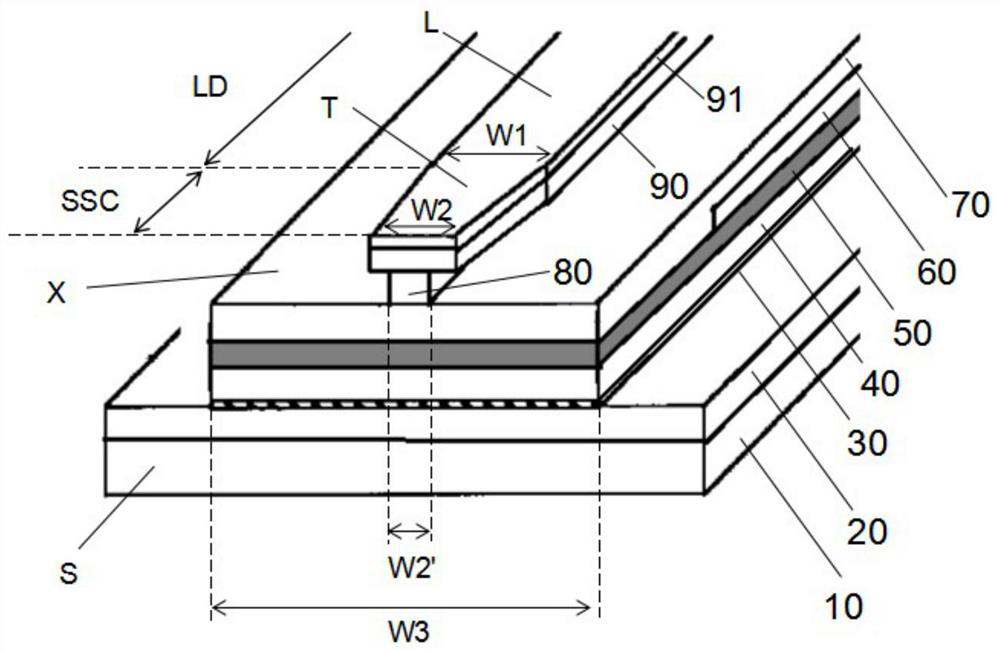
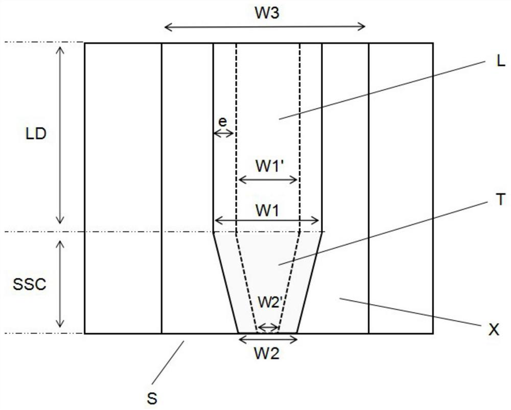
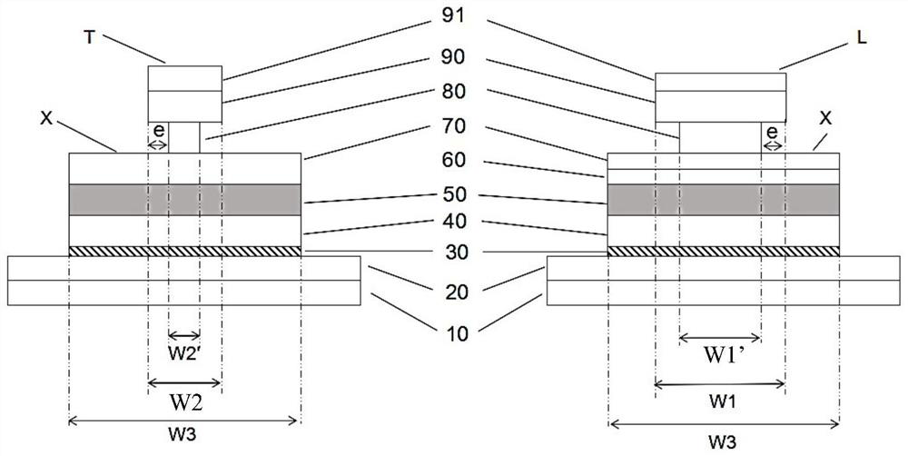
[0023] Specifically, according to some embodiments of the present invention, a method for manufacturing a semiconductor laser is provided, please refer to figure 1 , 2 And 3, take the InP-based material system as an example, but it is not limited thereto, it can also be other material systems such as silicon-based material systems, etc., the manufacturing method of the semiconductor laser includes the following steps:

[0024] (1) sequent...


PUM


Abstract

A semiconductor laser and a manufacturing method thereof, comprising the following steps: sequentially growing a buffer layer, a far-field reduction layer, a spacer layer, a quantum well material layer, and a grating layer on a substrate; and etching and removing the grating layer located in the mode spot converter region , make a grating from the grating layer in the laser area; grow a gap layer, an etching stop layer, a cladding layer and a contact layer in turn on the substrate with the grating; use the cladding layer and the contact layer to make an upper ridge waveguide, in which the laser area is The width of the upper ridge waveguide remains unchanged, and the width of the upper ridge waveguide in the mode spot converter area gradually decreases from the laser end to the light-emitting end of the device; after the etching stop layer other than the upper ridge waveguide is removed by selective wet etching, the etching stop layer is Lateral corrosion occurs under the upper ridge waveguide; the lower ridge waveguide is fabricated by etching from the gap layer of the mode spot converter region to the buffer layer. The mode-spot converter integrated on the semiconductor laser of the present invention can be realized by using a common contact photolithography process, which is beneficial to reduce the fabrication cost of the device.

Description

technical field [0001] The invention relates to the field of optoelectronic devices, in particular to a semiconductor laser and a manufacturing method thereof. Background technique [0002] The near-field spot of waveguides based on compound semiconductor materials is small and asymmetric, resulting in large and asymmetric far-field divergence angles. When the semiconductor device is directly coupled to the optical fiber, the coupling loss can be as high as 10dB due to the mismatch of the mode field between the optical fiber and the semiconductor waveguide, and the alignment tolerance is small, which undoubtedly increases the difficulty and cost of packaging. The mode-spot converter can almost adiabatically convert the asymmetric near-field distribution of the waveguide into a symmetrical input or output near-field, which can improve the coupling efficiency and coupling tolerance of active devices and optical fibers. The horizontal wedge waveguide speckle converter is a sim...

Claims


Application Information

Patent Timeline
Patent Type & Authority Patents(China)
IPC IPC(8): H01S5/10H01S5/34H01S5/02251
CPCH01S5/1014H01S5/34H01S5/02251
Inventor 梁松剌晓波
Owner INST OF SEMICONDUCTORS - CHINESE ACAD OF SCI
Why Eureka
Try Eureka