
LPDDR substrate design method, LPDDR substrate and electronic equipment

A design method and substrate technology, applied in the direction of electrical components, printed circuits, printed circuit manufacturing, etc., can solve the problems of lead wire residue, etc., achieve the effect of centralized etching area, convenient inspection, and meet performance requirements and aesthetic requirements

Active Publication Date: 2020-06-05
SHENZHEN DEMINGLI ELECTRONICS
View PDF11 Cites 0 Cited by
  • Summary
  • Abstract
  • Description
  • Claims
  • Application Information

AI Technical Summary

Problems solved by technology

[0004] The main purpose of the present invention is to provide a method for designing an LPDDR substrate, aiming at solving the problem of residual wires after the etching of the LPDDR substrate

Method used


Image

  • LPDDR substrate design method, LPDDR substrate and electronic equipment
  • LPDDR substrate design method, LPDDR substrate and electronic equipment
  • LPDDR substrate design method, LPDDR substrate and electronic equipment

Examples


Embodiment Construction

[0031] It should be understood that the specific embodiments described here are only used to explain the present invention, not to limit the present invention.

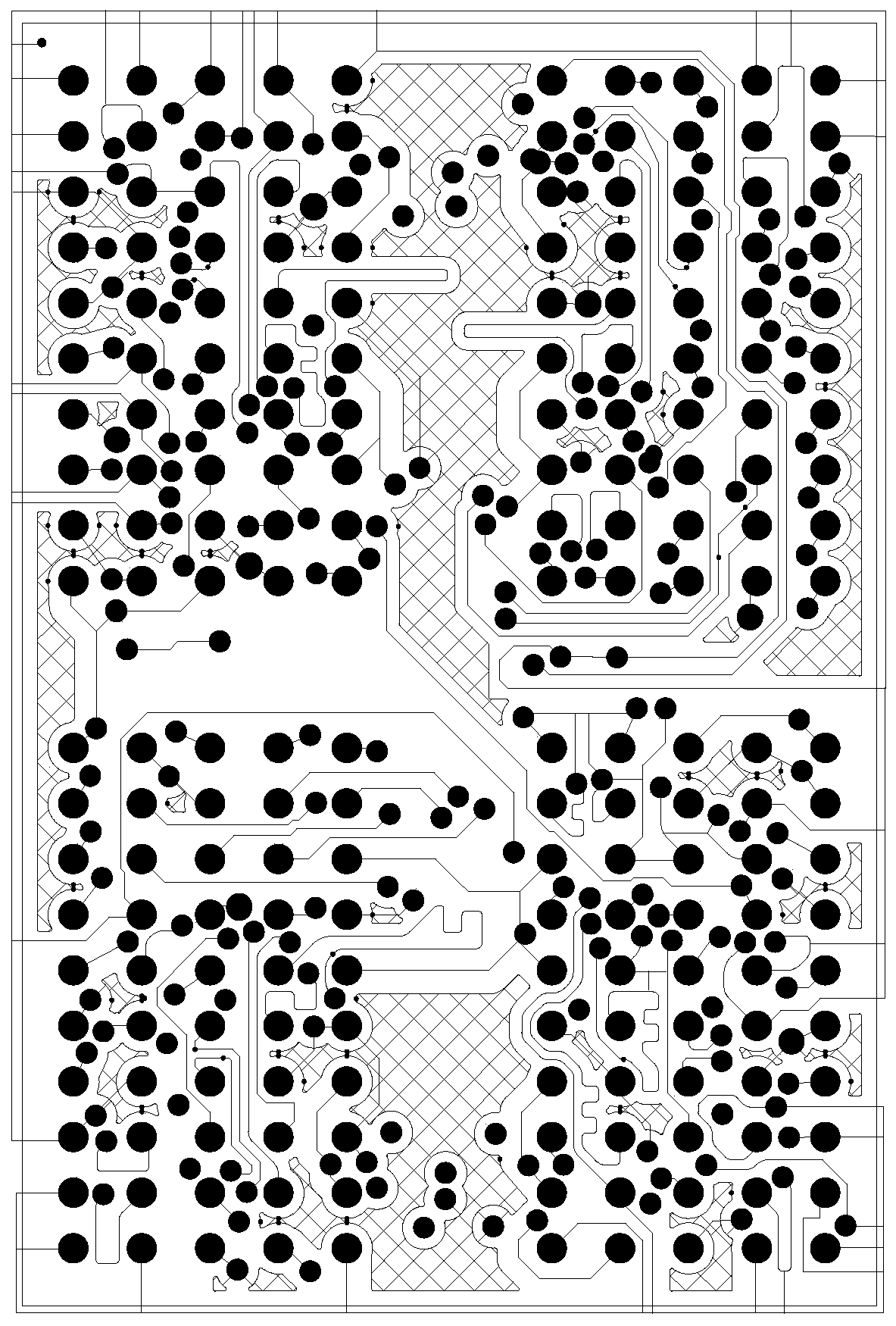
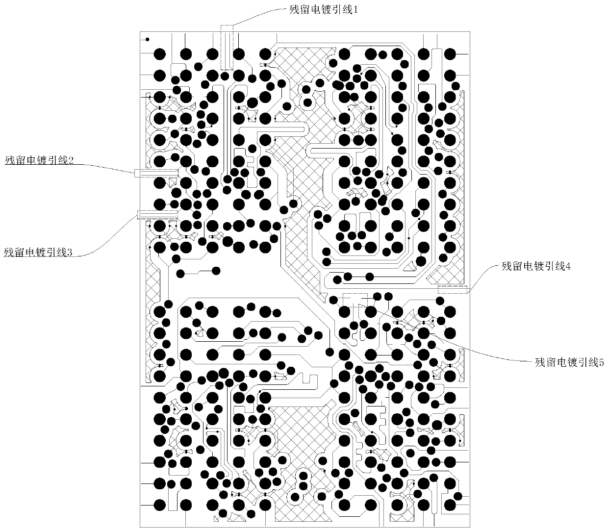
[0032] refer to Figure 5 , the present invention provides a method for designing an LPDDR substrate, comprising:

[0033] S1: Determining the chip packaging area 4 on the LPDDR substrate;

[0034] S2: A first etching area 1 and a second etching area 2 are respectively provided in the adjacent areas at both ends of the chip packaging area 4, wherein the first etching area 1 and the second etching area 2 are both used for setting the first electroplating lead 3, The first electroplating lead 3 is electrically connected to the circuit network to be electroplated on the LPDDR substrate.

[0035] In the embodiment of the present invention, the basic design process of the PCB board is as follows: the first step is the preliminary preparation, including the preparation of the component library and the schematic diagram; t...


PUM

PropertyMeasurementUnit
widthaaaaaaaaaa
widthaaaaaaaaaa

Abstract

The invention discloses an LPDDR substrate design method, an LPDDR substrate and electronic equipment. The LPDDR substrate design method comprises: determining a chip packaging region on the LPDDR substrate, and respectively arranging a first etching region and a second etching region in adjacent regions at two ends of the chip packaging region, wherein the first etching region and the second etching region are both used for arranging a first electroplating lead, and the first electroplating lead is electrically connected with a circuit network to be electroplated on the LPDDR substrate. According to the design method, the etching area of the electroplated lead is concentrated, later inspection is convenient, almost no residual lead tail exists, the defects caused by traditional substratedesign are well overcome, and the performance requirement and the attractiveness requirement of the LPDDR substrate are met.

Description

technical field [0001] The invention relates to the field of storage devices, in particular to an LPDDR substrate design method, an LPDDR substrate and electronic equipment. Background technique [0002] On the PCB board, copper is used to interconnect the components on the substrate. Although it is a good conductor material for forming the surface pattern of the PCB conductive path, if it is exposed to the air for a long time, it is easy to lose due to oxidation. Gloss, loses weldability due to exposure to corrosion. Therefore, electroplating techniques are used to protect copper traces, vias, and plated through holes. [0003] Copper printed lines need to be electroplated through leads. The traditional lead design is on the bottom of the substrate. Since it is necessary to etch outside the wafer chip as much as possible, a large number of circuits need to be lead out of the product, and the wiring is complicated. Such as figure 1 and 2 as shown, figure 2 The parts in...

Claims


Application Information

Patent Timeline
Patent Type & Authority Applications(China)
IPC IPC(8): H05K3/00H05K3/02H05K3/18
CPCH05K3/0002H05K3/022H05K3/18
Inventor 李虎谭少鹏
Owner SHENZHEN DEMINGLI ELECTRONICS
Learn More