Electronic device and method of manufacturing the same

An electronic component and a manufacturing method technology, which are applied in the field of electronic components with no-gap through holes and the manufacturing field thereof, can solve the problems of poor step coverage of contact holes, difficulty of no-gap through holes, etc.

Inactive Publication Date: 2020-06-09
NAN YA TECH
View PDF5 Cites 0 Cited by
  • Summary
  • Abstract
  • Description
  • Claims
  • Application Information

AI Technical Summary

Problems solved by technology

However, as scaling continues, void-free via formation becomes more difficult due to poor step coverage of contact holes with high aspect ratios

Method used


Image

  • Electronic device and method of manufacturing the same
  • Electronic device and method of manufacturing the same
  • Electronic device and method of manufacturing the same

Examples


preparation example Construction

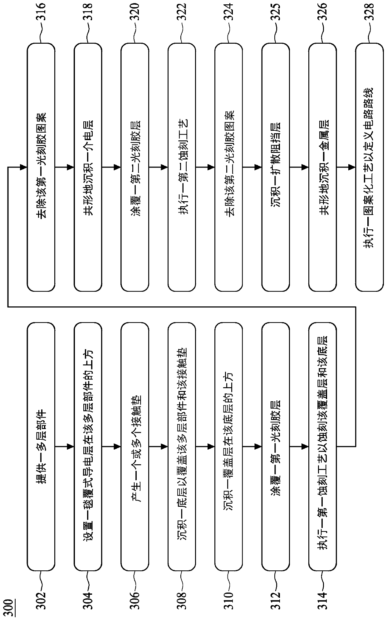
[0099] figure 2 It is a flowchart, and a method 300 of the electronic component 10 or 10a of the present disclosure is illustrated. Figure 3 to 20 It is a variety of manufacturing stages of the preparation method 300 of the electronic component 10 or 10a of some embodiments disclosed. Figure 3 to 20 The various stages figure 2 A schematic description of the manufacturing process. In the following description, Figure 3 to 20 The manufacturing step shown in the presentation corresponds to reference figure 2 Manufacturing steps in.

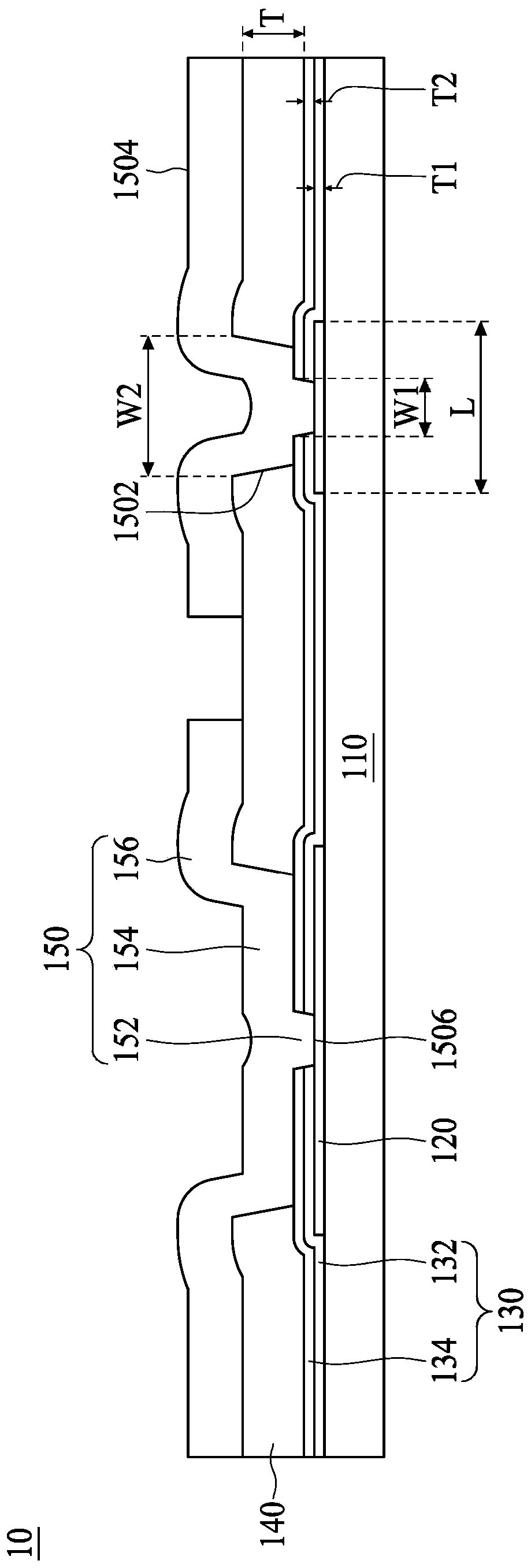
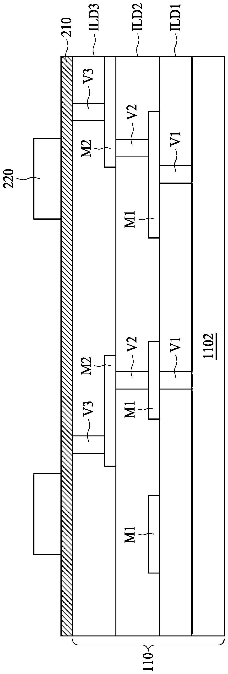
[0100] Refer image 3 ,according to figure 2 In step 302, a multilayer member 110 is provided. In some embodiments, the multilayer component 110 can include a primary component 1102, mainly composed of 1102 including one or more feature elements, such as transistors, resistors, capacitors, and diodes. In some embodiments, the multilayer member 110 may further include an interconnect structure including alternating stacks of wiring layers M1, M2, and thro...


PUM

PropertyMeasurementUnit
thicknessaaaaaaaaaa
thicknessaaaaaaaaaa

Abstract

The present disclosure provides an electronic device and a method of manufacturing the same. The electronic device includes a multilayer component, at least one contact pad, a passivation layer, a dielectric layer, and a metallic layer. The contact pad is disposed on the multilayer component, the passivation layer covers the multilayer component and the contact pad, and the dielectric layer is disposed on the passivation layer. The metallic layer penetrates through the dielectric layer and the passivation layer and is connected to the contact pad, and the metallic layer discretely tapers at positions of decreasing distance from the contact pad.

Description

Technical field [0001] The present disclosure advocates the priority and benefits of the US formal application No. 62 / 773, 823 and 2016 / 18, approved by 2011, 2011. The content of the formal application is incorporated herein by reference. [0002] The present disclosure relative to an electronic component and a method of manufacturing the same, and more particularly to an electronic component having a void-free Vias and a manufacturing method thereof. Background technique [0003] The semiconductor integrated circuit (IC) industry has developed rapidly. In the development process, the functional density of the integrated circuit is increased, and the geometry dimension is reduced. This process of scale reduction is usually accompanied by the increase in production efficiency, and the cost reduction. However, it also increases the complexity of processing and manufacturing integrated circuits, and in order to achieve these advances, the development of related technologies is also ...

Claims


Application Information

Patent Timeline
Patent Type & Authority Applications(China)
IPC IPC(8): H01L21/768H01L23/522
CPCH01L21/76897H01L23/5226H01L24/02H01L23/3157H01L2224/0235H01L2224/0236H01L2224/02313H01L2224/0239H01L2224/02331H01L2924/00012H01L2924/01029H01L2924/01013H01L2924/01022H01L2924/04941H01L2924/01073H01L2924/04953H01L2924/059H01L2924/0475H01L2924/00014H01L2924/0474H01L23/3171
Inventor 林育廷王茂盈施信益吴鸿谟丁永德
Owner NAN YA TECH
Why Eureka
Try Eureka