Method for producing thin film

A thin-film manufacturing method and thin-film technology, which are applied in semiconductor/solid-state device manufacturing, coating, gaseous chemical plating, etc., can solve problems such as corrosion of aluminum and other metals, film quality deterioration, and step coverage problems.

Pending Publication Date: 2021-03-26
SOULBRAIN CO LTD
View PDF13 Cites 0 Cited by
  • Summary
  • Abstract
  • Description
  • Claims
  • Application Information

AI Technical Summary

Problems solved by technology

Therefore, compared with the chemical vapor deposition (CVD, chemical vapor deposition) process that mainly uses the gas phase reaction, the atomic layer deposition (ALD, atomic layer deposition) process using the surface reaction is more used, but in achieving 100% step coverage (step coverage) is still a problem
[0005] In addition, titanium tetrachloride (TiCl 4 ), at this time, process by-products such as chlorides will remain in the manufactured film, which will induce the corrosion of metals such as aluminum, and cause the deterioration of film quality due to the formation of non-volatile by-products

Method used


Image

  • Method for producing thin film
  • Method for producing thin film
  • Method for producing thin film

Examples


Embodiment 1 to 7

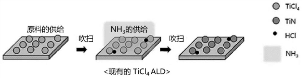
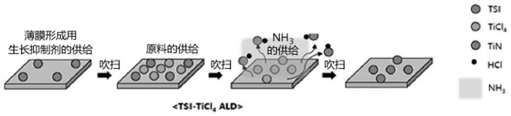
[0102] Prepare the growth inhibitor for thin film formation and TiCl as Ti-based thin film precursor described in Table 1 below. 4 . The prepared growth inhibitor for thin film formation was filled in a tank, and supplied to a vaporizer heated to 150° C. at a flow rate of 0.05 g / min by LMFC (Liquid Mass Flow Controller) at room temperature. After 3 seconds of injecting the growth inhibitor for thin film formation vaporized into the vapor phase in the evaporator into the deposition chamber loaded with the substrate, argon gas was supplied at 3000 sccm for 6 seconds and purged with argon gas. At this time, the pressure in the reaction chamber was controlled to 1.3 Torr. Then, the prepared TiCl 4 It was put into another tank, and was supplied to another evaporator heated to 150° C. at a flow rate of 0.05 g / min using LMFC (Liquid Mass Flow Controller) at normal temperature. TiCl vaporized into the vapor phase in the evaporator 4 After being put into the deposition chamber for ...

experiment example

[0110] 1) Deposition evaluation

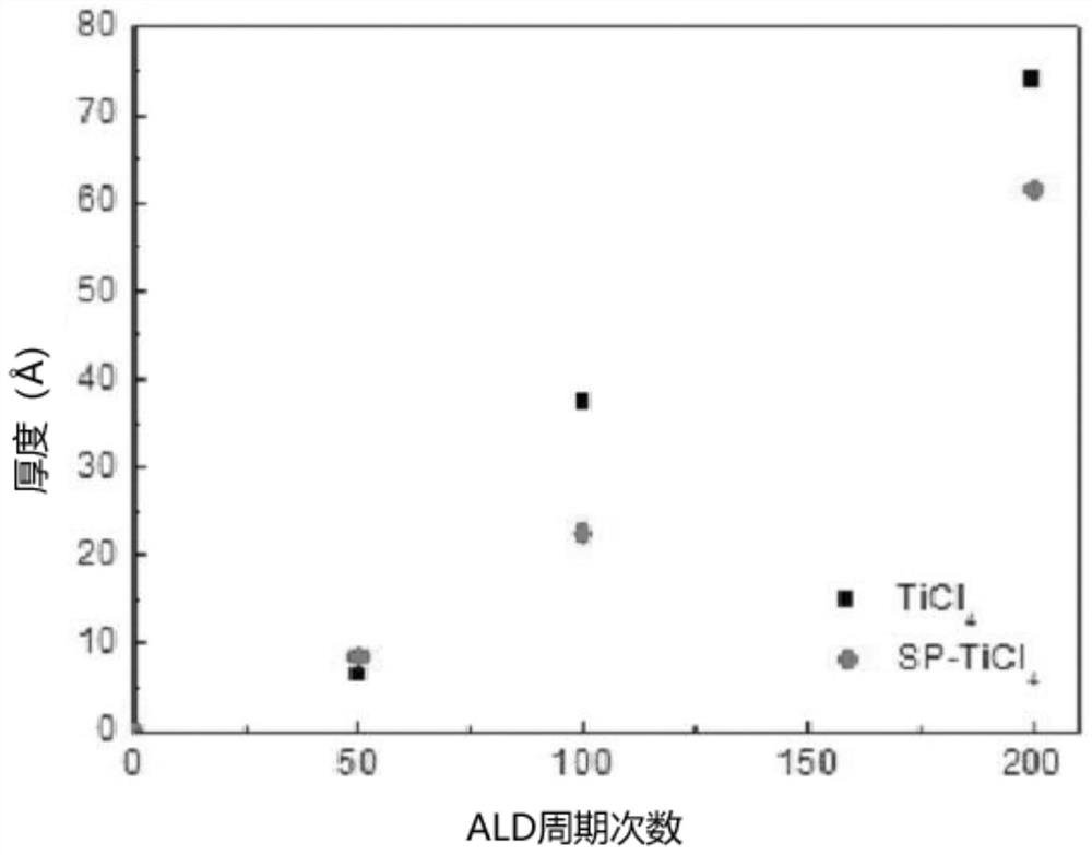
[0111] Referring to Table 2 below, Example 1 in which 2-chloro-2-methylbutane was used as a growth inhibitor for film formation was compared with Comparative Example 1 in which it was not included. As a result, the deposition rate is / Cycle, compared with Comparative Example 1, the deposition rate was reduced by more than 55.5%. It could be confirmed that the remaining Examples 2 to 7 also had deposition rates of similar values ​​to Example 1. In addition, it was confirmed that Comparative Examples 2 and 3, which did not use the growth inhibitor for thin film formation of the present invention but used pentane or cyclopentane, had the same deposition rate as Comparative Example 1. At this time, a decrease in the deposition rate indicates a change in the CVD deposition characteristics to the ALD deposition characteristics, and thus can be used as an indicator of improvement in the step coverage characteristics.

[0112] Table 2

[0113] ...


PUM

PropertyMeasurementUnit
densityaaaaaaaaaa
solubility (mass)aaaaaaaaaa

Abstract

The present invention relates to a method for producing a thin film, the method comprising: a step (i) for adsorbing a growth inhibitor for forming a thin film represented by chemical formula 1 onto the surface of a substrate; and ii) adsorbing a Ti-based thin film precursor onto the surface of the substrate to which the growth inhibitor for thin film formation has been adsorbed. According to thepresent invention, by suppressing side reactions, reducing the growth rate of a thin film, and removing process by-products in the thin film, the step coverage rate and the thickness uniformity of thethin film are greatly improved even when the thin film is formed on a substrate having a complex structure. Chemical formula 1: AnBmXo, where A is carbon or silicon, B is hydrogen or an alkyl group having 1 to 3 carbon atoms, X is halogen, n is an integer of 1 to 15, o is an integer of 1 or more, and m is 0 to 2n+1.

Description

technical field [0001] The present invention relates to a thin film manufacturing method, and in more detail relates to appropriately reducing the growth rate of the thin film by suppressing side reactions, and preventing corrosion and deterioration by removing process by-products in the thin film, even when a thin film is formed on a substrate with a complex structure. A thin film manufacturing method that greatly improves the step coverage and the uniformity of the thickness of the thin film. Background technique [0002] The integration level of storage and non-storage semiconductor devices is increasing day by day. As their structures become more and more complex, step coverage becomes more and more important when depositing various thin films on substrates. [0003] The semiconductor thin film is formed of metal nitride, metal oxide, metal silicide, or the like. The metal nitride thin films include titanium nitride (TiN), tantalum nitride (TaN), zirconium nitride (ZrN)...

Claims


Application Information

Patent Timeline
Patent Type & Authority Applications(China)
IPC IPC(8): C23C16/455C23C16/34C23C16/52
CPCC23C16/45527C23C16/34C23C16/52H01L21/28562H01L21/76841C23C16/045C23C16/45534C23C16/405H01L21/0228H01L21/02205H01L21/02312H01L21/324H01L21/67017C23C16/44H01L2924/01022C23C16/45544C23C16/303H01L21/28568
Inventor 延昌峰郑在善边惠兰宋泰浩金素贞李锡宗
Owner SOULBRAIN CO LTD
Why Eureka
Try Eureka