

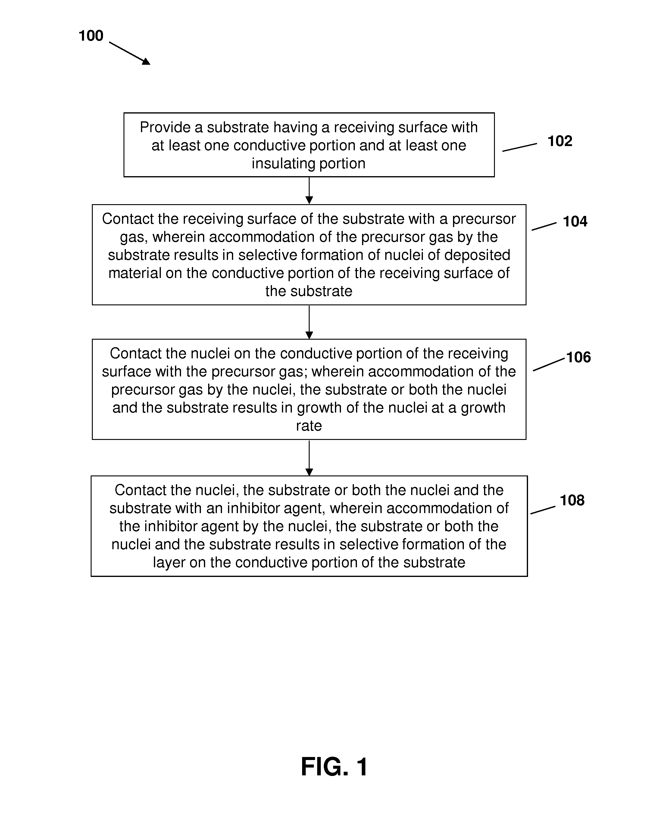
Use of an inhibitor molecule in chemical vapor deposition to afford deposition of copper on a metal substrate with no deposition on adjacent sio2 substrate
a technology of inhibitor molecule and chemical vapor deposition, which is applied in the direction of chemical vapor deposition coating, coating, metallic material coating process, etc., can solve the problems of device failure, reliability problem, and difficult patterning of cu, and achieve the effect of reducing the growth rate of nuclei
- Summary
- Abstract
- Description
- Claims
- Application Information
AI Technical Summary
Benefits of technology
Problems solved by technology
Method used
Image

Examples
example 1
Surface-Selective Chemical Vapor Deposition of Copper Films Through the Use of a Molecular Inhibitor
Abstract
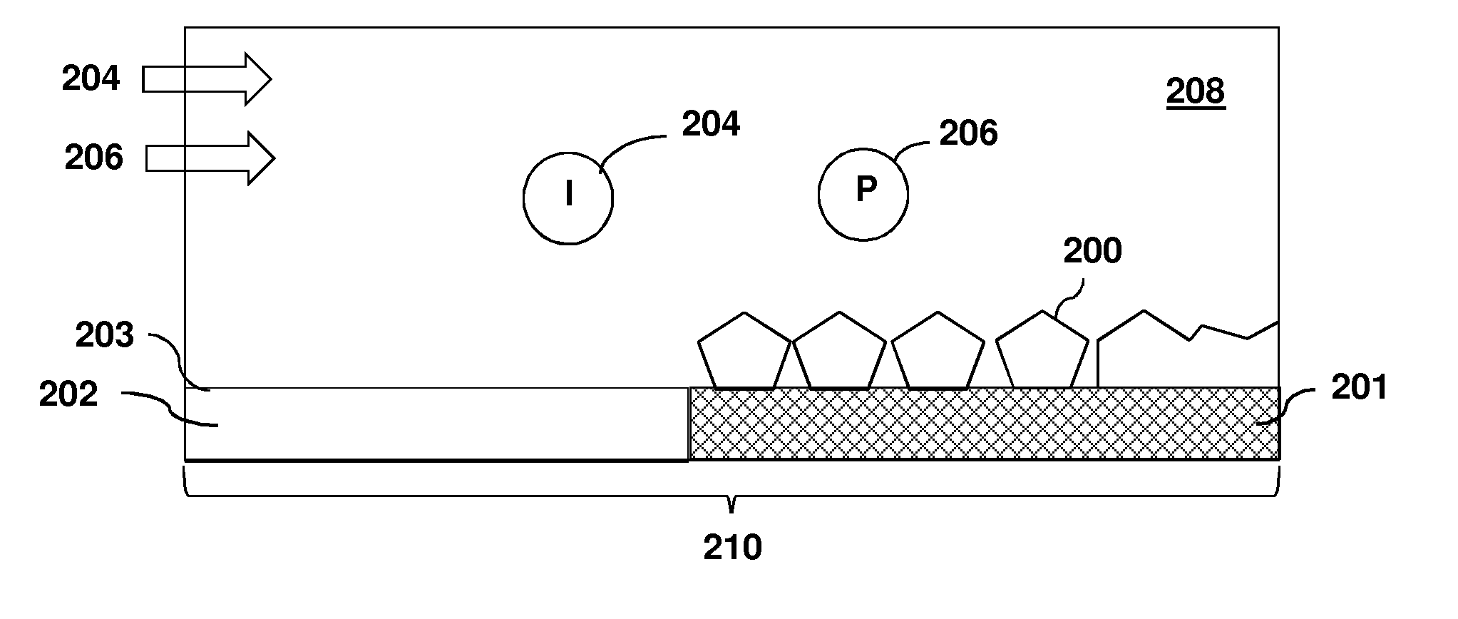
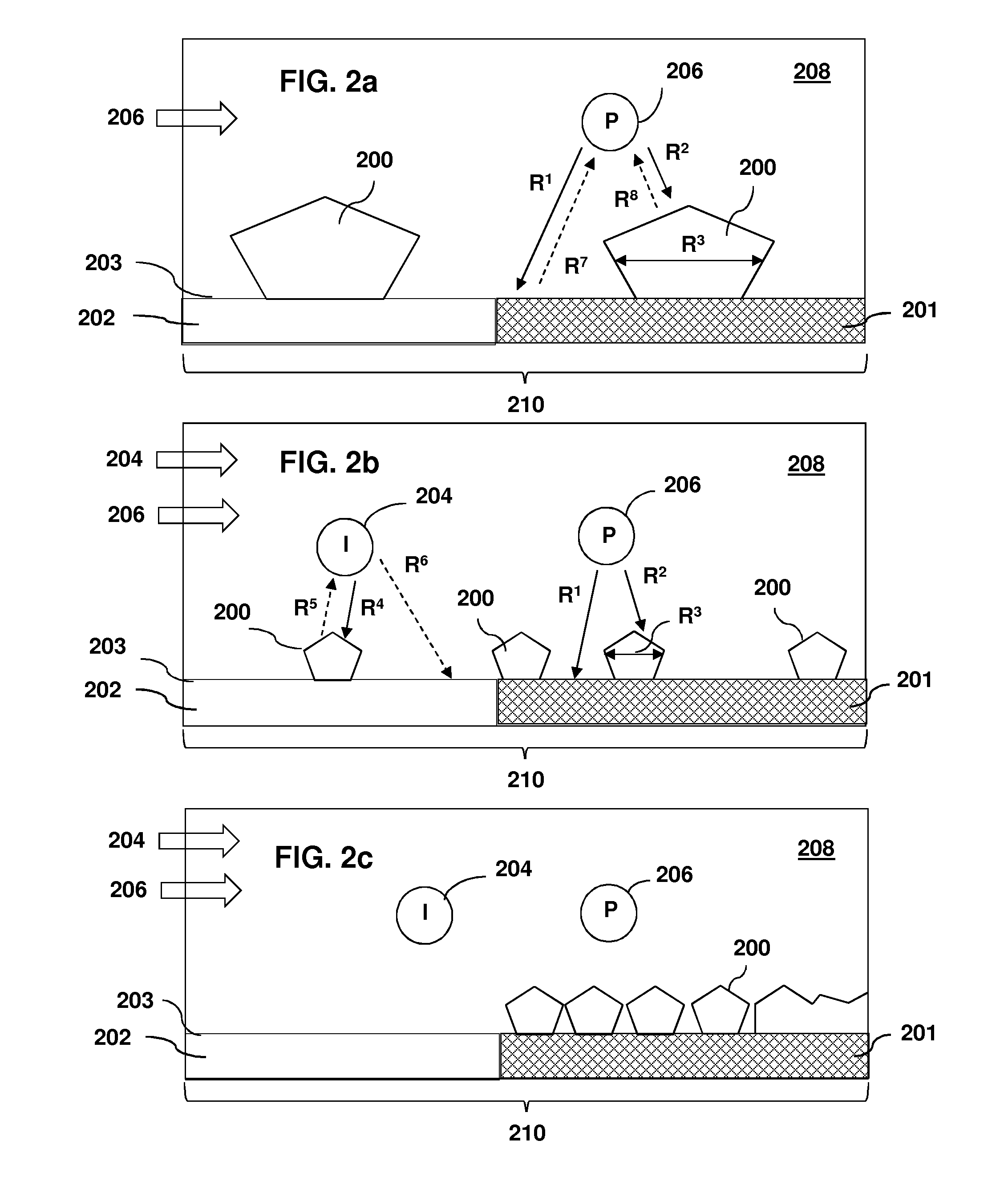
[0080]This Example reports a simple process for the selective deposition of copper films on RuO2, while no Cu nucleation occurs on thermal SiO2 or porous carbon doped oxide (CDO). Using the precursor Cu(hfac)VTMS, selectivity is attained by adding a co-flow of excess VTMS to act as a growth inhibitor. With precursor alone, 52 nm of Cu grows on RuO2; on CDO or on thermal SiO2, nucleation is delayed such that 41 or 1.3 nm are deposited, respectively. Repeating the experiment with the co-flow of VTMS affords a 12 nm thick Cu film on RuO2 with roughness of 1.8 nm. But on CDO or thermal SiO2, the Cu deposition is only 0.10 or ˜0.04 nm, respectively. AFM scans of the CDO and SiO2 surfaces are identical to the bare substrates. The small quantity of Cu that is deposited must be finely distributed, presumably on defect sites; it can be etched to below the RBS detection limit using a co...
example 2
Use of an Inhibitor Molecule in Chemical Vapor Deposition to Afford Deposition of Copper on a Metal Substrate with No Deposition on Adjacent SiO2 Substrate, i.e., Perfect Surface-Selective Growth
Abstract
[0133]This Example reports a one-step process for selective deposition of Cu on a metallic surface, air-exposed Ru, while no Cu growth at all occurs on adjacent SiO2 surfaces. Selectivity was attained by co-flowing a growth inhibitor, vinyl trimethyl silane (VTMS) along with the stream of the deposition precursor, Cu(hfac)VTMS. With precursor alone, for a growth temperature of 100° C. and a growth time of 30 min., a 52 nm thick Cu film with 6.8 nm rms roughness was formed on air-exposed Ru, and 1×10¹⁵ Cu atoms / cm2 (as measured by RBS) were deposited on SiO2. Nucleation on SiO2 consisted of islands with an areal density of ˜9×108 cm−2 and rms roughness 2.3 nm. The experiment was then repeated, but co-flowing 4 mTorr of VTMS growth inhibitor along with the precursor. In this case, the ...
example 3
Chemical Vapor Deposition of Copper: Use of a Molecular Inhibitor to Afford Uniform Nanoislands or Smooth Films
Abstract
[0154]This example reports a method to control the surface morphology of thin copper films during growth by chemical vapor deposition from the precursor Cu(hfac)VTMS. A molecular inhibitor—an additive that modifies the surface attachment kinetics but does not decompose and contribute impurity atoms to the film—is added during the nucleation and / or growth stages of the film. Here we show that the reaction byproduct VTMS can serve as such an inhibitor. If the inhibitor is added during the nucleation stage, when bare substrate surface is still exposed, the inhibitor greatly reduces the rate of coalescence and promotes the formation of a large density of uniformly-sized copper islands. Alternatively, if the film is allowed to nucleate in the absence of the inhibitor, subsequent addition of the inhibitor leads to a continuous copper film that is remarkably smooth on the ...
PUM
| Property | Measurement | Unit |
|---|---|---|
| temperature | aaaaa | aaaaa |
| thickness | aaaaa | aaaaa |
| conductivity | aaaaa | aaaaa |
Abstract
Description
Claims
Application Information