Method for making wear-resistant dielectric layer

A manufacturing method and dielectric layer technology, applied in the manufacture of circuits, electrical components, semiconductor/solid-state devices, etc., to achieve the effect of improving yield and reliability, and improving step coverage

Inactive Publication Date: 2008-11-26
TOUCH MICRO SYST TECH
View PDF4 Cites 0 Cited by
  • Summary
  • Abstract
  • Description
  • Claims
  • Application Information

AI Technical Summary

Problems solved by technology

[0005] Therefore, the main purpose of the present invention is to provide a method for making a wear-resistant dielectric layer, so as to overcome the unsolvable problems in the prior art

Method used


Image

  • Method for making wear-resistant dielectric layer
  • Method for making wear-resistant dielectric layer
  • Method for making wear-resistant dielectric layer

Examples


Embodiment Construction

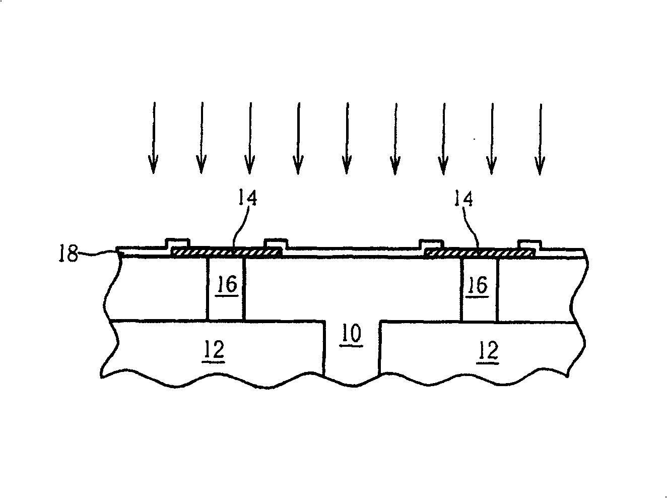
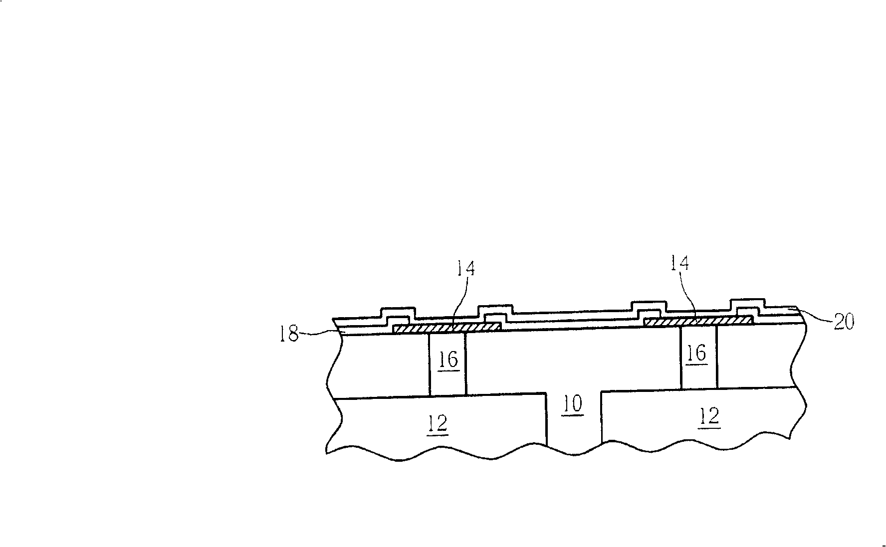
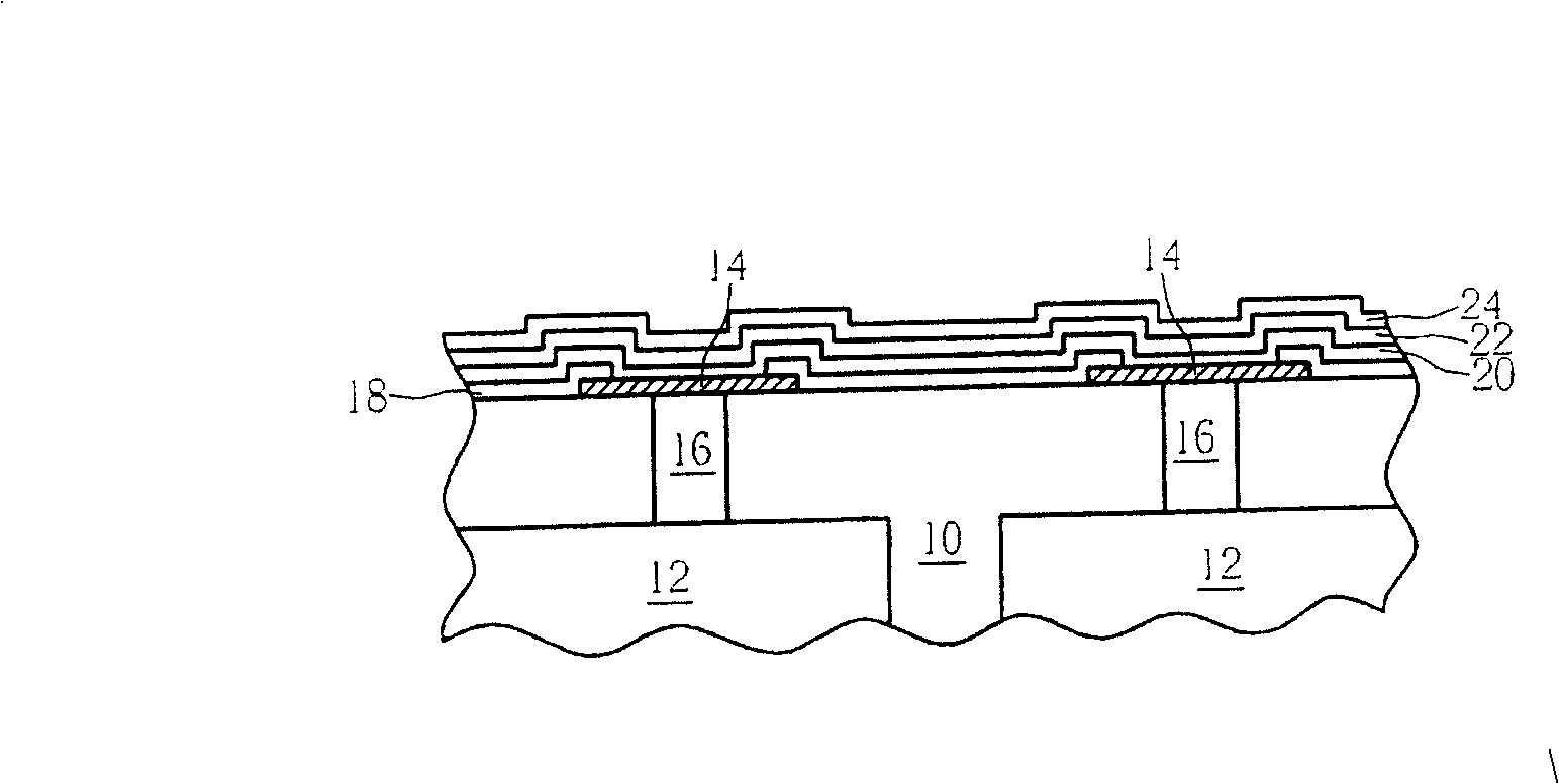
[0019] Please refer to Figure 1 to Figure 8 . Figure 1 to Figure 8 It is a schematic diagram of a method for fabricating a wear-resistant dielectric layer in a preferred embodiment of the present invention. Such as figure 1 As shown, a substrate 10 is first provided, and the substrate 10 includes a plurality of elements 12, and a plurality of connection pads 14 are arranged on the surface of the substrate 10, and are electrically connected to the elements 12 by a plug 16, wherein the elements 12 are semiconductor elements or microelectromechanical components, etc. In addition, the surface of the substrate 10 further includes a surface dielectric layer 18 . Then carry out a surface treatment process to the surface dielectric layer 18, to remove the organic pollutants and particles attached to the surface dielectric layer 18, and increase the distance between the surface dielectric layer 18 and the subsequently formed dielectric layer (not shown). Adhesion between. In this...


PUM

PropertyMeasurementUnit
thicknessaaaaaaaaaa
thicknessaaaaaaaaaa
angleaaaaaaaaaa

Abstract

The invention firstly provides a substrate comprising plural connection pads, successively at least makes a plasma auxiliary chemical vapour deposition process to deposit a dielectric layer on the substrate surface, where the vapour deposition process is made in a high frequency-low frequency plasma alternating mode, and finally makes an anisotropic etching process to form plural openings in the dielectric layer, where these openings correspond to the connection pads and side wall of each opening is inclined outward.

Description

technical field [0001] The invention relates to a method for making a dielectric layer, in particular to a method for making a wear-resistant dielectric layer by using a high-frequency-low-frequency plasma interlaced manner to perform a plasma-enhanced chemical vapor deposition process. Background technique [0002] In the manufacture of semiconductor components and MEMS components, the dielectric layer is mainly used to provide insulation and protection functions. Therefore, depending on the application, the selection of the dielectric layer must take into account the size of the dielectric constant, structural strength and dielectric layer. The stress problem of itself and other materials, etc. Generally, materials commonly used as dielectric layers mainly include silicon oxide and silicon nitride, among which silicon oxide is often used as The material of the gate dielectric layer emphasizes dielectric properties. On the other hand, silicon nitride is often used as a pro...

Claims


Application Information

Patent Timeline
Patent Type & Authority Patents(China)
IPC IPC(8): H01L21/31H01L21/318
Inventor 赖委舜胡书华黄冠瑞潘锦昌许渊钦
Owner TOUCH MICRO SYST TECH
Why Eureka
Try Eureka