Ferroelectric domain defined series two-dimensional photovoltaic cell and preparation method thereof
A technology of photovoltaic cells and ferroelectric domains, applied in the field of two-dimensional semiconductor photovoltaic devices, can solve problems such as complex processes and difficult control of doping levels, and achieve the effect of reducing energy consumption
- Summary
- Abstract
- Description
- Claims
- Application Information
AI Technical Summary
Problems solved by technology
Method used
Image

Examples
Embodiment example 1
[0037] The specific steps for implementing Case 1 are as follows:
[0038] 1) Preparation of insulating substrate
[0039] The insulating substrate is a silicon substrate covered with silicon dioxide;
[0040] 2) Preparation and transfer of two-dimensional semiconductors of bipolar transition metal compounds
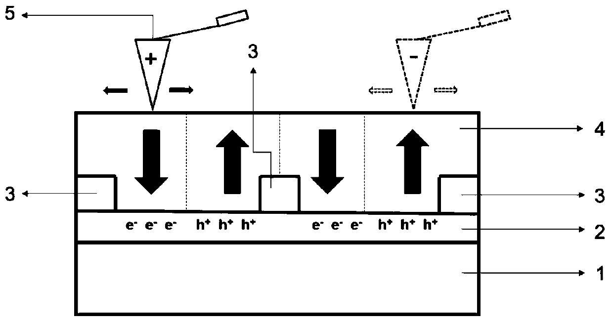
[0041] Bipolar transition metal compound two-dimensional semiconductor 8 nm MoTe by mechanical exfoliation 2 transferred to an insulating substrate.
[0042] 3) Metal electrode preparation
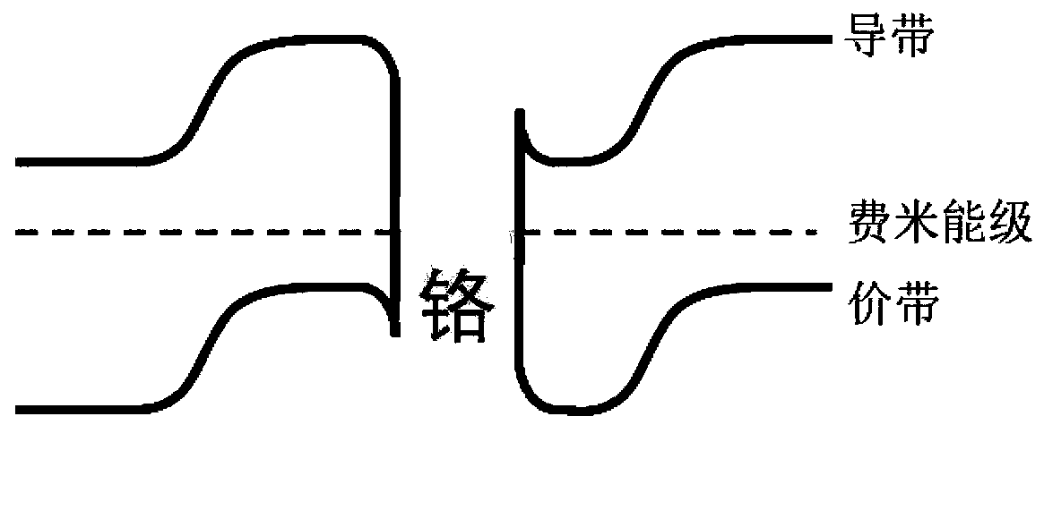
[0043] The metal electrode 3 is prepared by using ultraviolet lithography or electron beam exposure technology combined with thermal evaporation and lift-off technology. The electrodes are chromium and gold, the thickness of chromium is 10 nm, and the thickness of gold is 20 nm.
[0044] 4) Preparation of ferroelectric functional layer
[0045] The polyvinylidene fluoride-based ferroelectric functional layer was prepared by spin coating on the prepared device, and annealed at 1...
Embodiment example 2
[0048] The specific steps for implementing Case 2 are as follows:
[0049] 1) Preparation of insulating substrate
[0050] The insulating substrate is a silicon substrate covered with silicon dioxide;
[0051] 2) Preparation and transfer of two-dimensional semiconductors of bipolar transition metal compounds
[0052] Bipolar transition metal compound two-dimensional semiconductor 10 nm MoTe by mechanical exfoliation 2 transferred to an insulating substrate.
[0053] 3) Metal electrode preparation
[0054] The metal electrode 3 is prepared by using ultraviolet lithography or electron beam exposure technology combined with thermal evaporation and lift-off technology. The electrodes are chromium and gold with a thickness of 10 nm and 20 nm, respectively.
[0055] 4) Preparation of ferroelectric functional layer
[0056] The polyvinylidene fluoride-based ferroelectric functional layer was prepared by spin coating on the prepared device, and annealed at 135°C for 2 hours to e...
Embodiment example 3
[0059] The specific steps for implementing Case 3 are as follows:
[0060] 1) Preparation of insulating substrate
[0061] The insulating substrate is a silicon substrate covered with silicon dioxide;
[0062] 2) Preparation and transfer of two-dimensional semiconductors of bipolar transition metal compounds
[0063] Bipolar transition metal compound two-dimensional semiconductor 12 nm MoTe by mechanical exfoliation 2 transferred to an insulating substrate.
[0064] 3) Metal electrode preparation
[0065] The metal electrode 3 is prepared by using ultraviolet lithography or electron beam exposure technology combined with thermal evaporation and lift-off technology. The electrodes are chromium and gold with a thickness of 10 nm and 20 nm, respectively.
[0066] 4) Preparation of ferroelectric functional layer
[0067] The polyvinylidene fluoride-based ferroelectric functional layer was prepared by spin coating on the prepared device, and annealed at 135°C for 2 hours to e...
PUM
| Property | Measurement | Unit |
|---|---|---|
| thickness | aaaaa | aaaaa |
| thickness | aaaaa | aaaaa |
| thickness | aaaaa | aaaaa |
Abstract
Description
Claims
Application Information
 - R&D
- Intellectual Property
- Life Sciences
- Materials
- Tech Scout
- Unparalleled Data Quality
- Higher Quality Content
- 60% Fewer Hallucinations
Browse by: Latest US Patents, China's latest patents, Technical Efficacy Thesaurus, Application Domain, Technology Topic, Popular Technical Reports.
© 2025 PatSnap. All rights reserved.Legal|Privacy policy|Modern Slavery Act Transparency Statement|Sitemap|About US| Contact US: help@patsnap.com