Ferroelectric field regulated and controlled two-dimensional material PN junction photoelectric detector and preparation method thereof
A photodetector, two-dimensional material technology, applied in the fields of electric solid device, semiconductor/solid state device manufacturing, circuit, etc., can solve the problems of slow light response and low response rate, and achieve fast response speed, high response rate and sensitivity. high effect
- Summary
- Abstract
- Description
- Claims
- Application Information
AI Technical Summary
Problems solved by technology
Method used
Image

Examples
Embodiment 1
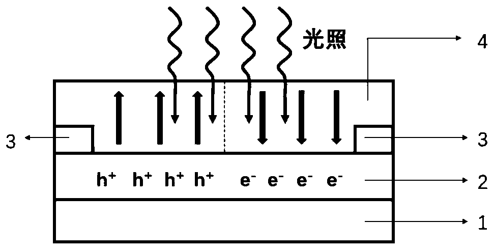
[0053] In this embodiment, a MoTe with ferroelectric domain regulation is provided 2 In-plane PN junction, the structural section of the device is as figure 1 shown.
[0054] The detector includes a substrate 1 , a two-dimensional semiconductor 2 , a metal electrode 3 , and a ferroelectric functional layer 4 from bottom to top.
[0055] In embodiment 1, substrate 1 is a silicon / silicon dioxide substrate, and the thickness of silicon dioxide is 285 nanometers; the two-dimensional semiconductor 2 is a two-dimensional material MoTe 2 , its thickness is 10 nanometers; metal electrode 3 is chromium / gold electrode, chromium 10 nanometers, gold 20 nanometers; Ferroelectric function layer 4 is ferroelectric polymer P (VDF-TrFE), and its thickness is 50 nanometers.
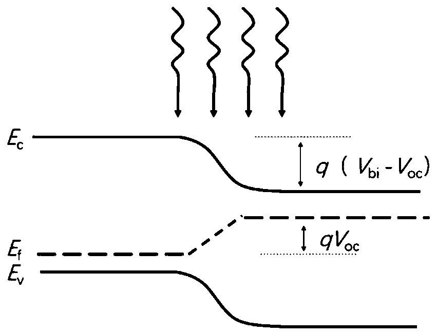
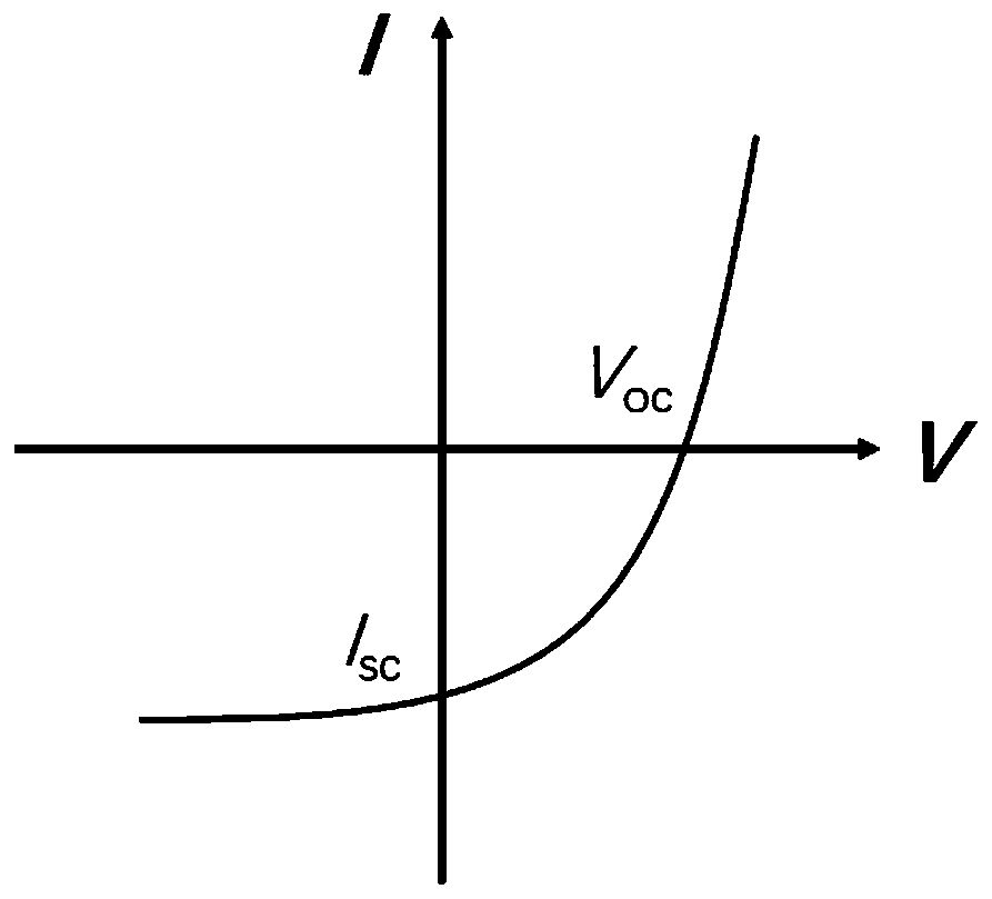
[0056] Figure 4 The current-voltage relationship of the in-plane PN junction photodetector formed by regulating the two-dimensional material for the ferroelectric material under illumination has an obvious photocurrent...
Embodiment 2
[0058] In this embodiment, a MoTe with ferroelectric domain regulation is provided 2 In-plane PN junction, the structural section of the device is as figure 1 shown.
[0059] The detector includes a substrate 1 , a two-dimensional semiconductor 2 , a metal electrode 3 , and a ferroelectric functional layer 4 from bottom to top.
[0060] In embodiment 2, substrate 1 is a silicon / silicon dioxide substrate, and the thickness of silicon dioxide is 285 nanometers; the two-dimensional semiconductor 2 is a two-dimensional material MoTe 2 , its thickness is 12 nanometers; metal electrode 3 is chromium / gold electrode, chromium 10 nanometers, gold 20 nanometers; Ferroelectric function layer 4 is ferroelectric polymer P (VDF-TrFE), and its thickness is 50 nanometers.
[0061] Figure 5 The current-voltage relationship of the in-plane PN junction photodetector formed by regulating the two-dimensional material for the ferroelectric material under illumination has an obvious photocurrent...
Embodiment 3
[0063] In this embodiment, a MoTe with ferroelectric domain regulation is provided 2 In-plane PN junction, the structural section of the device is as figure 1 shown.
[0064] The detector includes a substrate 1 , a two-dimensional semiconductor 2 , a metal electrode 3 , and a ferroelectric functional layer 4 from bottom to top.
[0065] In embodiment 3, substrate 1 is a silicon / silicon dioxide substrate, and the thickness of silicon dioxide is 285 nanometers; the two-dimensional semiconductor 2 is a two-dimensional material MoTe 2 , its thickness is 15 nanometers; metal electrode 3 is chromium / gold electrode, chromium 10 nanometers, gold 20 nanometers; Ferroelectric function layer 4 is ferroelectric polymer P (VDF-TrFE), and its thickness is 50 nanometers.
[0066] Image 6 The current-voltage relationship of the in-plane PN junction photodetector formed by regulating the two-dimensional material for the ferroelectric material under illumination has an obvious photocurrent ...
PUM
| Property | Measurement | Unit |
|---|---|---|
| thickness | aaaaa | aaaaa |
| thickness | aaaaa | aaaaa |
| thickness | aaaaa | aaaaa |
Abstract
Description
Claims
Application Information
 - R&D
- Intellectual Property
- Life Sciences
- Materials
- Tech Scout
- Unparalleled Data Quality
- Higher Quality Content
- 60% Fewer Hallucinations
Browse by: Latest US Patents, China's latest patents, Technical Efficacy Thesaurus, Application Domain, Technology Topic, Popular Technical Reports.
© 2025 PatSnap. All rights reserved.Legal|Privacy policy|Modern Slavery Act Transparency Statement|Sitemap|About US| Contact US: help@patsnap.com