Three-dimensional memory manufacturing method and three-dimensional memory

A manufacturing method and memory technology, applied in semiconductor/solid-state device manufacturing, electric solid-state devices, semiconductor devices, etc., can solve the problem of difficult control of gate seam etching depth, achieve precise control of etching precision, reduce etching Depth, the effect of reducing machining errors

Active Publication Date: 2020-06-23
YANGTZE MEMORY TECH CO LTD
View PDF7 Cites 4 Cited by
  • Summary
  • Abstract
  • Description
  • Claims
  • Application Information

AI Technical Summary

Problems solved by technology

[0005] The invention provides a method for manufacturing a three-dimensional memory and a three-dimensional memory to overcome the problem that the etching depth of the grid seam is difficult to control in the related art

Method used


Image

  • Three-dimensional memory manufacturing method and three-dimensional memory
  • Three-dimensional memory manufacturing method and three-dimensional memory
  • Three-dimensional memory manufacturing method and three-dimensional memory

Examples


Embodiment Construction

[0060] The specific embodiments of the present invention will be described in detail below with reference to the accompanying drawings. It should be understood that the specific embodiments described here are only used to illustrate and explain the present invention, and the present invention is not limited to the following specific embodiments.

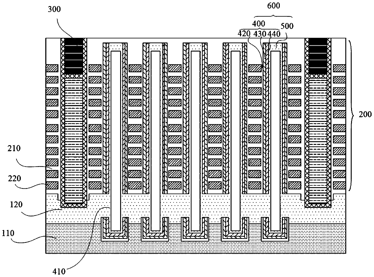
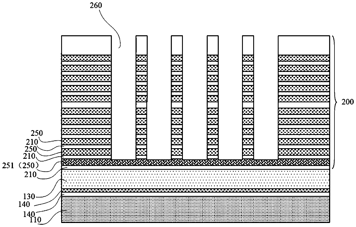
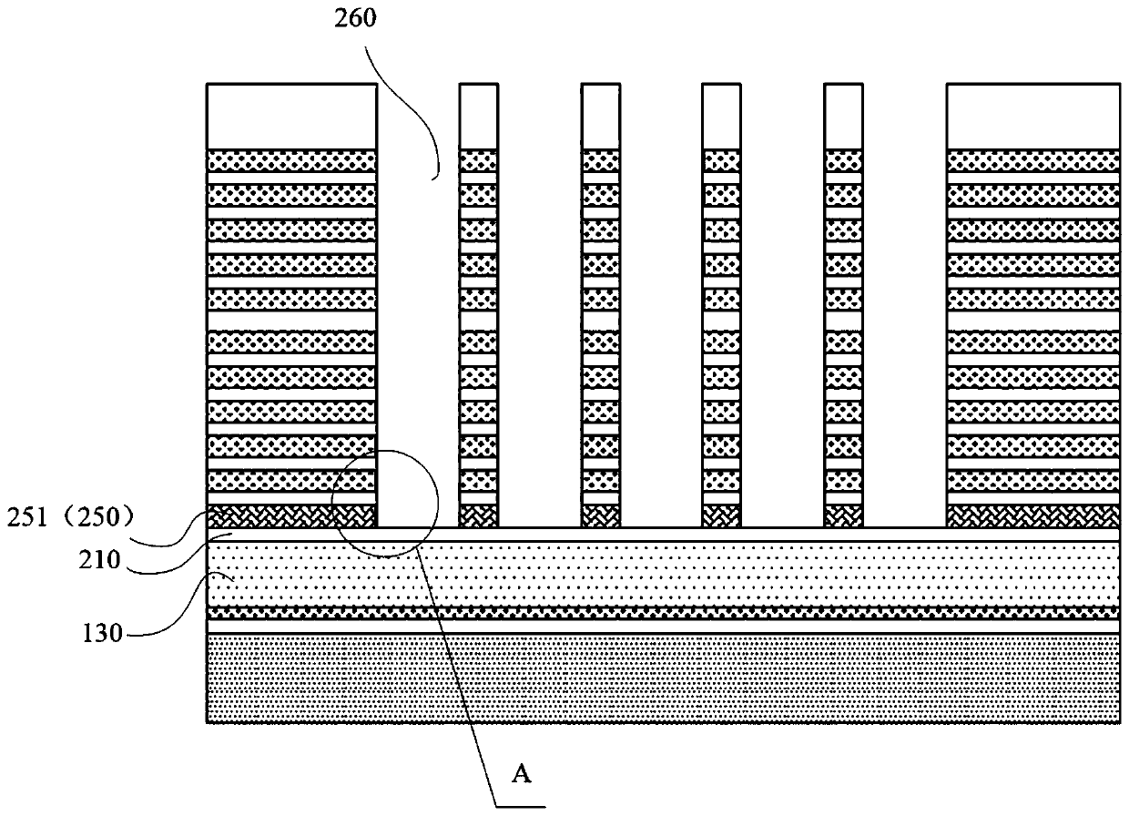
[0061] At present, in the manufacturing process of a three-dimensional memory, in order to electrically connect the channel layer in the channel hole to the common source contact in the gate slit, it is usually chosen to first provide a sacrificial layer between the stack structure and the substrate, and use The gate slit is etched so that the gate slit extends into the sacrificial layer, thereby removing the sacrificial layer and the functional layer in the sacrificial layer, and exposing the channel layer from the sidewall of the channel hole, and then passing through the stack structure and the substrate A semiconductor substrate is n...


PUM


Abstract

The invention provides a three-dimensional memory manufacturing method and a three-dimensional memory, and the method comprises: forming a semiconductor structure, and enabling a stack structure of the semiconductor structure to be provided with a first structural hole with the bottom located at an etching stop layer; removing the etching stop layer at the bottom of the first structure hole, and exposing the insulating layer at the bottom of the etching stop layer; further extending the bottom of the first structure hole into the sacrificial layer; removing the sacrificial layer to form a sacrificial gap; forming a second substrate in the sacrificial gap; and forming a common source contact in the first structural hole. An etching stop layer is arranged in a stack structure of the three-dimensional memory, the etching stop layer can be used as a stop layer for etching the first structural hole, and the etching depth in the last process step can be reduced due to the fact that the position of the etching stop layer in the stack structure is determined, so that the machining error is reduced, the etching precision is accurately controlled, and the bottom of the first structural holecan be just located in the sacrificial layer and cannot be too deep or too shallow.

Description

Technical field [0001] The present invention relates to three-dimensional memory technology, in particular to a three-dimensional memory manufacturing method and a three-dimensional memory. Background technique [0002] With the rapid development of technologies such as big data, cloud computing, and the Internet of Things, the requirements for memory integration and storage density have also increased. Traditional two-dimensional planar memories have been unable to meet actual needs and are gradually being replaced by three-dimensional memories. [0003] In the related art, a three-dimensional memory includes a substrate and a stack structure stacked on the substrate. The stack structure is provided with a channel hole and a gate slit penetrating the substrate, the channel structure is provided in the channel hole, and the gate slit is provided There is a common source contact; and the channel layer of the channel structure can be exposed from the sidewall of the channel hole and ...

Claims


Application Information

Patent Timeline
Patent Type & Authority Applications(China)
IPC IPC(8): H01L27/11563H01L27/11565H01L27/11578H01L21/308
CPCH10B41/23H10B41/20H10B43/23H10B43/20
Inventor 吴林春杨永刚周文犀
Owner YANGTZE MEMORY TECH CO LTD
Why Eureka
Try Eureka