Negative luminescence cold shield (NLCS) with microlenses to magnify the effective area of sparsely populated negative luminescence regions and method of fabrication

a negative luminescence and cold shield technology, applied in the field of cold shields for ir focal plane arrays, can solve the problems of limiting system performance, affecting device processing, and causing excessive noise, and reducing the effective area of sparsely populated negative luminescence regions, so as to reduce reduce the cost effect of nlcs , the effect of reducing the total diode area

Active Publication Date: 2009-01-06
TELEDYNE SCI & IMAGING
View PDF3 Cites 1 Cited by
  • Summary
  • Abstract
  • Description
  • Claims
  • Application Information

AI Technical Summary

Benefits of technology

[0014]The present invention provides a cost-effective NLCS and method of fabrication for reducing the total diode area with minimal effect on device processing. This is accomplished with an array of microlenses on the backside of a semiconductor substrate transparent to thermal IR radiation whose front side is sparsely populated with negative luminescence (NL) regions. Each region contains an IR absorbing semiconductor with one or more diodes to produce the negative luminescence within the IR semiconductor material. These regions may, for example, be formed using an epitaxial structure or by mounting a thinned NL semiconductor on a substrate. Each microlens, properly positioned and sized, creates a magnified image at the FPA of the relatively small NL region corresponding to that microlens. From the point of view of the FPA, this magnified image makes each microlens and the entire microlensed area of the substrate appear cold.
[0015]The microlenses are fabricated on the backside of the substrate away from the devices, preferably prior to or after device processing, and thus the microlenses and their fabrication have minimal negative effect on device processing. This ensures high quality devices that maintain NL efficiency without excessive power consumption. To further simplify processing, the microlenses may be fabricated with a planar or “Fresnel” geometry, thus reducing the required etching depth.
[0016]The NLCS is designed and configured to cover the solid angle outside the incident optics and not otherwise cold-shielded by a conventional cold shield. The microlenses are preferably designed and arranged so that their images of their NL regions cover only a predetermined solid angle occupied by the FPA thereby reducing the diode area required for the NLCS and thus reducing the power required for its use.

Problems solved by technology

Without appropriate shielding the remainder of the field of view at ambient temperature will irradiate the FPA with unwanted photons, creating excess noise and, potentially, saturating its output.
Cold shields are essential to operation of high-sensitivity IR FPAs, but their need for cooling (both because they must be cold not to radiate significantly and because they themselves, being large, absorb radiation from the outside which must be extracted through the inefficiency of the system cooler) and awkward size and shape typically complicate packaging and system optics adding substantially to cost and size, and possibly power.
For simple systems, this may be only 80-90% and may actually limit the system performance.
The principal drawback to this NLCS is the high power consumption of the ambient-temperature, large-area (typically >6 cm2) semiconductor device needed to provide efficient shielding (or partial shielding, if used in conjunction with a small, relatively convenient conventional cold shield).
Thus, reducing the total area of these interfacial regions proportionately reduces the likelihood of including a current-enhancing defect.
However, because the minority carriers need to diffuse farther to get to the now more remote junction, some of them may recombine by radiative or other mechanisms before reaching the diode, thus the NL efficiency may be degraded unless the individual diodes are placed within a minority carrier diffusion length of each other.
Such three dimensional architectures greatly complicate semiconductor processing and may compromise NLCS performance.
This diffractive spreading reduces the NL efficiency at the FPA, and may need to be offset by deeper, larger a focal concentrators to insure that the spreading does not render the percentage of radiation suppression inadequate at the FPA.

Method used


Image

  • Negative luminescence cold shield (NLCS) with microlenses to magnify the effective area of sparsely populated negative luminescence regions and method of fabrication
  • Negative luminescence cold shield (NLCS) with microlenses to magnify the effective area of sparsely populated negative luminescence regions and method of fabrication
  • Negative luminescence cold shield (NLCS) with microlenses to magnify the effective area of sparsely populated negative luminescence regions and method of fabrication

Examples


Embodiment Construction

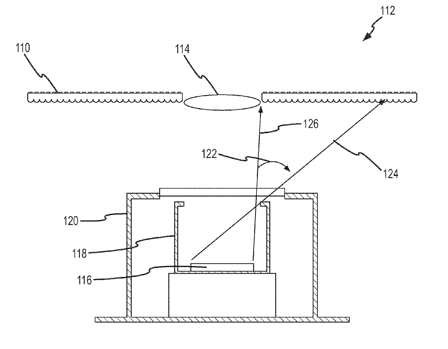
[0027]The present invention provides a cost-effective NLCS and method of fabrication for reducing the total diode area with minimal effect on device processing.

[0028]As shown in FIGS. 4a and 4b, a NLCS 80 is sparsely populated with NL regions 81, each region consisting of one or more diodes 82 formed in NL semiconductor material 84-, e.g. MWIR or LWIR HgCdTe, InSb, PbSnTe, PbSnSe, InAsSb, MWIR or LWIR strained layer superlattice semiconductors, or any of a variety of MWIR and LWIR semiconductors known to those in the art, on an IR transparent substrate 86 with a refractive index n, suitably 2.7 to 4. The NL semiconductor material has a refractive index near that of the substrate sufficient to minimize interfacial reflections, <2% being typical. These NL regions may, for example, be formed using an epitaxial structure or by mounting a thinned NL semiconductor on a substrate.

[0029]The NL regions 81 are connected across the NLCS by a conducting layer 88 comprised preferably of a wider ...


PUM


Abstract

An array of microlenses magnifies the effective negative luminescence regions of a sparsely populated NLCS so that the NLCS appears cold to a FPA. This approach reduces the total diode area with minimal effect on device processing. The microlenses are fabricated on the backside of the substrate away from the devices, either prior to or after device processing. This ensures high quality devices that maintain NL efficiency without negatively impacting power consumption.

Description

FIELD OF THE INVENTION[0001]This invention relates to cold shields for IR focal plane arrays (FPAs) and more specifically to the use of microlenses to magnify the effective area of sparsely populated negative luminescence regions in a negative luminescence cold shield (NLCS).DESCRIPTION OF THE RELATED ART[0002]All objects, because they are warm (at ambient or room temperature), emit large amounts of thermal radiation in the infrared (IR) spectral regions; and what they do not emit they reflect from their warm surroundings. Because the atmosphere is transparent in two of these IR regions, the MWIR region (˜3 μm to ˜5) and the LWIR region (8-14 μm), these regions may be used conveniently for IR or “thermal” imaging by IR focal plane arrays (FPAs). IR FPAs serve mainly to sense the small differences in thermal radiation intensity from an ambient temperature scene by converting to electrical signals those incident scene photons focused on the FPA by the system optics. To do this with hi...

Claims


Application Information

Patent Timeline
Patent Type & Authority Patents(United States)
IPC IPC(8): G01J5/20
CPCH01L27/14627H01L27/14649H01L27/14685H04N5/33
Inventor TENNANT, WILLIAM E.
Owner TELEDYNE SCI & IMAGING
Why Eureka
Try Eureka