MEMS package carrier plate stack-up structure and manufacturing method thereof

A technology for encapsulating carrier boards and manufacturing methods, which is applied in chemical/electrolytic methods to remove conductive materials, multilayer circuit manufacturing, and printed circuit manufacturing. There are many technical difficulties and other problems to achieve the effect of reducing product scrap rate, facilitating mass production, and simple production methods

Active Publication Date: 2020-06-23
JIANGSU PROVISION ELECTRONICS CO LTD
View PDF4 Cites 0 Cited by
  • Summary
  • Abstract
  • Description
  • Claims
  • Application Information

AI Technical Summary

Problems solved by technology

[0002] At present, the manufacturing methods of the three-layer MEMS package carrier board stacking structure commonly used in the circuit board manufacturing industry are mainly the following two: manufacturing method 1), the copper clad laminate is laminated with copper foil on one side after the inner layer circuit is completed; but Since the PP semi-cured resin has a certain fluidity, the PP semi-cured resin gradually solidifies and generates stress during the hot pressing process, which leads to uneven force on one side of the PCB board, and then warpage.
Production method 2), use special materials as fixed plates, and build layers on this basis; although this method can improve the warping problem, the process is relatively complicated, with many technical difficulties and high production costs, which is not conducive to large-scale mass production

Method used


Image

  • MEMS package carrier plate stack-up structure and manufacturing method thereof
  • MEMS package carrier plate stack-up structure and manufacturing method thereof

Examples


Embodiment 1

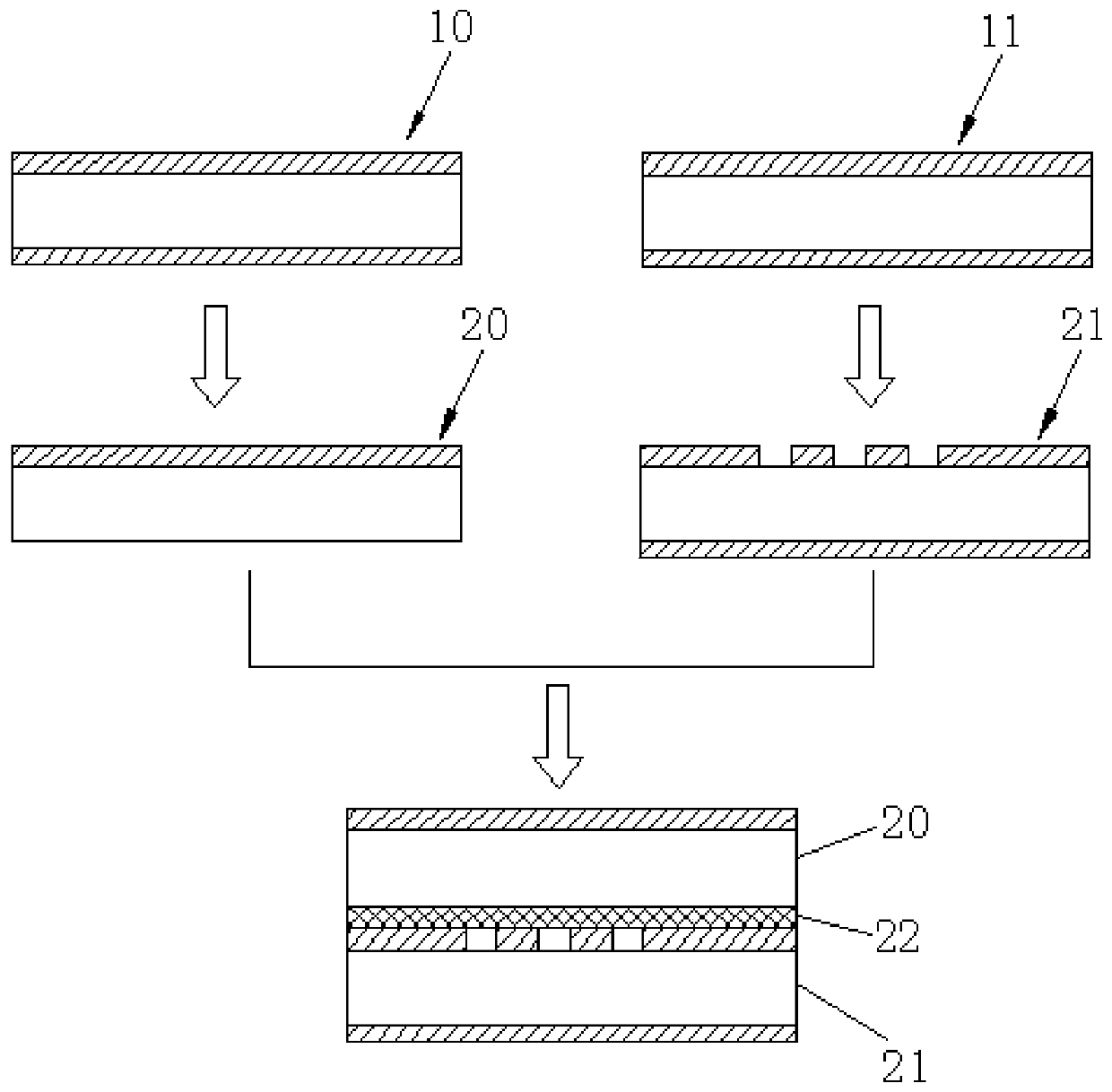
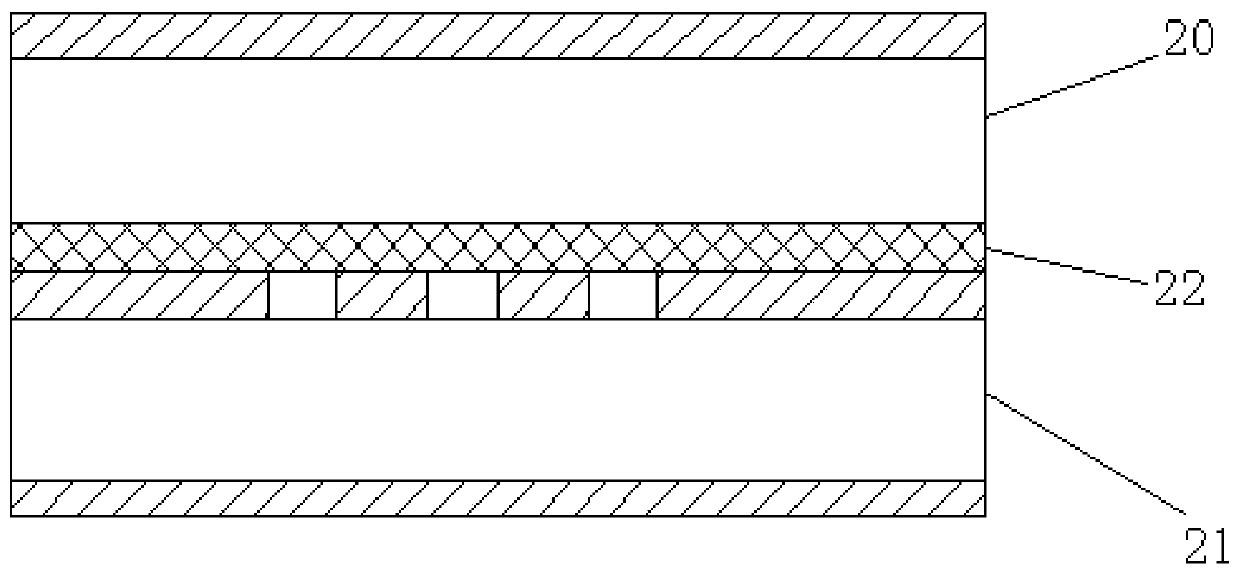
[0031] Please refer to the attached figure 1 And attached figure 2 As shown in FIG. 2 , they are the fabrication flow chart of the stacked structure of the MEMS package substrate and the schematic diagram of the enlarged structure, respectively, according to the present invention.

[0032] The invention provides a method for manufacturing a MEMS packaging carrier stack structure, comprising the following steps:

[0033] Step 1), prepare two double-sided copper-clad substrates I, and define them as copper-clad substrate A10 and copper-clad substrate B11 respectively;

[0034] Step 2), processing the copper-clad substrate A10 to obtain a single-sided copper-clad substrate 20, and the specific processing method is: 2a), performing surface treatment on the copper-clad substrate A10, that is, the copper-clad substrate A Oxidation and dirt removal on the surface of the two-layer copper foil to enhance the adhesion between the dry film and the copper foil; 2b), laminating a layer ...


PUM


Abstract

The invention discloses an MEMS package carrier plate stack-up structure and a manufacturing method thereof. The manufacturing method comprises the following steps: preparing a copper-clad substrate Aand a copper-clad substrate B; processing the copper-clad substrate A to obtain a single-sided copper-clad substrate; processing the copper-clad substrate B to obtain a double-sided copper-clad substrate II with a single-sided circuit; and sequentially stacking, aligning and laminating the single-sided copper-clad substrate, a PP sheet and the double-sided copper-clad substrate II to form an MEMSpackaging substrate stack-up structure with a pseudo four-layer plate structure. The manufacturing method of the MEMS package carrier plate stack-up structure is relatively simple and easy to operate, the warping problem is well solved, the quality of a circuit board product is ensured, and the production cost is reduced.

Description

technical field [0001] The invention relates to the technical field of circuit board manufacturing, and specifically provides a MEMS packaging carrier board stack structure and a manufacturing method thereof. Background technique [0002] At present, the manufacturing methods of the three-layer MEMS package carrier board stacking structure commonly used in the circuit board manufacturing industry are mainly the following two: manufacturing method 1), the copper clad laminate is laminated with copper foil on one side after the inner layer circuit is completed; but Since the PP semi-cured resin has a certain fluidity, the PP semi-cured resin gradually solidifies and generates stress during the hot pressing process, which leads to uneven force on one side of the PCB board and warpage. Production method 2), use special materials as fixed plates, and build layers on this basis; although this method can improve the warping problem, the process is relatively complicated, with many ...

Claims


Application Information

Patent Timeline
IPC IPC(8): H05K3/46H05K3/06
CPCH05K3/06H05K3/4611
Inventor 马洪伟刘浩宗芯如
Owner JIANGSU PROVISION ELECTRONICS CO LTD
Why Eureka
Try Eureka