

A semiconductor laser cos alloy strength detection device and detection method
A technology for alloy strength and detection devices, which is applied in the direction of measuring devices, mechanical devices, instruments, etc., can solve the problems that the strength of COS removal is not easy to control, the mold strips cannot be fixed accurately, and the result error is large. It is not easy to solve the problem Control, operation and inspection are convenient, reliable and cost-effective
- Summary
- Abstract
- Description
- Claims
- Application Information
AI Technical Summary
Problems solved by technology
Method used
Image

Examples
Embodiment 1
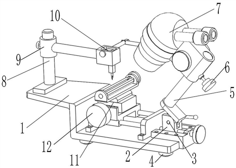
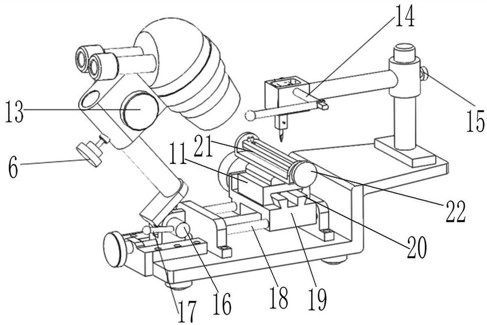
[0044] The translation mechanism can be the following structure, which includes a sliding rod 18 horizontally arranged on the base 1 along the front-rear direction, a sliding seat II 19 slidably installed on the sliding rod 18, and a dovetail guide rail horizontally arranged on the sliding seat II 19 along the left-right direction. 20 and the sliding seat I 11 slidably installed on the dovetail guide rail 20, and the fixing bar 21 is arranged on the sliding seat I 11. The sliding seat II 19 slides along the front and rear directions of the sliding rod 18 to realize the adjustment of the position of the die bar 31 in the front and rear directions.
Embodiment 2
[0046] The height adjustment mechanism can be the following structure, which includes a guide rod II 8 vertically arranged on the base 1, a sliding sleeve 9 slidably installed on the guide rod II 8, and a sliding sleeve 9 that is screwed on the sliding sleeve 9 for relatively the sliding sleeve 9. The guide rod II 8 locks the fixed handle screw II 15, and the support 10 is connected with the sliding sleeve 9. After loosening the handle screw II 15, the support 10 can slide up and down along the guide rod II 8 through the sliding sleeve 9. After the height of the pressing needle 24 is adjusted in place, the position of the sliding sleeve 9 can be fixed by tightening the handle screw II 15. Fixing of the height position of the support 10.
Embodiment 3
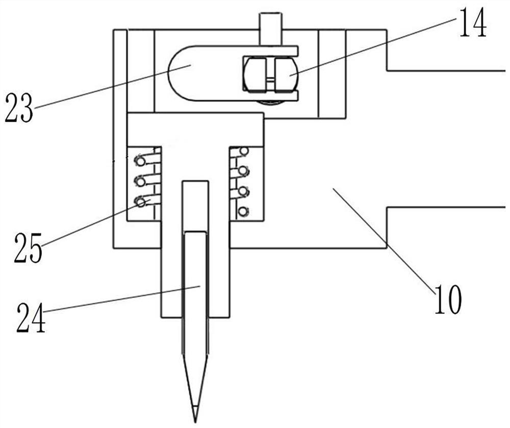
[0048] It may also include a positioning hole provided at the lower end of the mold bar 31 and a positioning protrusion 26 provided on the fixing bar 21 that matches the positioning hole. The positioning protrusion 26 is inserted into the positioning hole at the lower end of the mold bar 31 . The positioning protrusion 26 can improve the positioning accuracy of the mold bar 31 when it is mounted on the fixing bar 21 .
PUM
 Abstract
Description
Claims
Application Information