A kind of oled display panel and its manufacturing method
A technology for a display panel and a manufacturing method, which is used in the manufacture of semiconductor/solid-state devices, identification devices, instruments, etc., can solve the problems of large bending degree, unfavorable wiring, circuit breakage, etc., and achieves good flexibility, easy bending and stretching, preventing dislocation effect
- Summary
- Abstract
- Description
- Claims
- Application Information
AI Technical Summary
Problems solved by technology
Method used
Image
Examples
no. 1 example
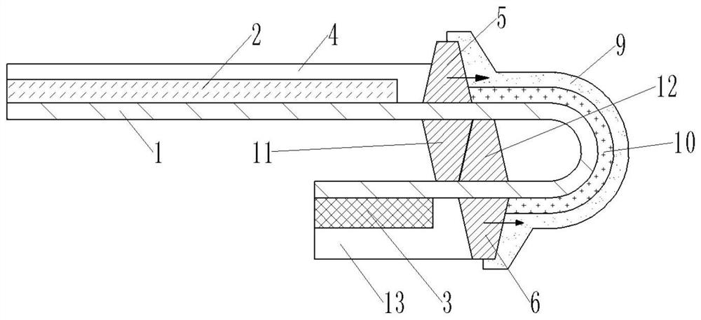
[0039] figure 1 is a cross-sectional view of an OLED display panel according to the present invention, figure 2 yes figure 1 Sectional view of the bent state. Such as figure 1 , 2 As shown, the OLED display panel includes a display area, a bending area and a driving area arranged in sequence. The display area includes a flexible substrate 1 ; a display device 2 sequentially formed on the flexible substrate 1 ; and a sealing layer 4 sealing the display device 2 . The display device 2 may be an organic light-emitting diode (Organic Light-Emitting Diode, OLED) or a quantum dot light-emitting diode (Quantum Dot Light-Emitting Diode, QLED), etc., which is not limited in the present invention.
[0040] In the bending region, the flexible substrate 1 has a first spacer 5 and a second spacer 6 spaced apart on its first surface, and a third spacer 11 and a second spacer 6 spaced apart on its second surface. Four spacers 12 . The spacer is made of polyethylene, polystyrene, poly...
no. 2 example
[0046] image 3 is a cross-sectional view of an OLED display panel according to the present invention, Figure 4 yes image 3 Sectional view of the bent state. Such as image 3 , 4 As shown, its structure is basically similar to that of the first embodiment, the only difference is that the first organic layer 10 is formed on the second surface between the third spacer 11 and the second spacer 12, and the second organic layer 9 is in direct contact with the first surface at the recessed portion.
[0047] In this embodiment, the bending strength of the first organic layer is also greater than that of the second organic layer, and its material is also the same as that of the first embodiment.
[0048] And, when the driving region is bent below the second surface, the side walls of the third spacer 11 and the fourth spacer 12 abut against each other, and the third spacer 11 and the fourth spacer 12 abut against each other. The top surface of one of the fourth spacers 12 rest...
no. 3 example
[0050] Figure 5 is a cross-sectional view of an OLED display panel according to the present invention, Figure 6 yes Figure 5 Sectional view of the bent state. Such as Figure 5 , 6 As shown, its structure is basically similar to that of the first embodiment, the only difference is that the first spacer 5 and the third spacer 11 are combined into one through the through hole 16 in the flexible substrate 1 to form a spacer 14, and the second spacer 5 The second spacer 6 and the fourth spacer 12 are combined into one through the bump 17 to form the spacer 15 , so that the spacer can be prevented from being peeled off from the flexible substrate 1 .
[0051] In this embodiment, the bending strength of the first organic layer is also greater than that of the second organic layer, and its material is also the same as that of the first embodiment. And the arrangement of the first organic layer 10 can also be arranged on the second surface similarly to the second embodiment (n...
PUM
 Abstract
Description
Claims
Application Information


