Circuit board device, preparation method thereof and electronic equipment

A technology of circuit boards and substrates, applied in circuits, electrical components, electrical solid devices, etc., can solve problems such as easy short circuits in packaged chips, and achieve the effect of solving short circuits and stable and reliable connections

Active Publication Date: 2020-06-30
维沃移动通信(重庆)有限公司
View PDF4 Cites 1 Cited by
  • Summary
  • Abstract
  • Description
  • Claims
  • Application Information

AI Technical Summary

Problems solved by technology

[0004] The invention discloses a circuit board device, a preparation method thereof, and electronic equipment, which can solve the problem that a short circuit is likely to occur in the process of packaging a packaged chip on a circuit board

Method used


Image

  • Circuit board device, preparation method thereof and electronic equipment
  • Circuit board device, preparation method thereof and electronic equipment
  • Circuit board device, preparation method thereof and electronic equipment

Examples


Embodiment Construction

[0040] In order to make the purpose, technical solution and advantages of the present invention clearer, the technical solution of the present invention will be clearly and completely described below in conjunction with specific embodiments of the present invention and corresponding drawings. Apparently, the described embodiments are only some of the embodiments of the present invention, but not all of them. Based on the embodiments of the present invention, all other embodiments obtained by persons of ordinary skill in the art without making creative efforts belong to the protection scope of the present invention.

[0041] The technical solutions disclosed by various embodiments of the present invention will be described in detail below in conjunction with the accompanying drawings.

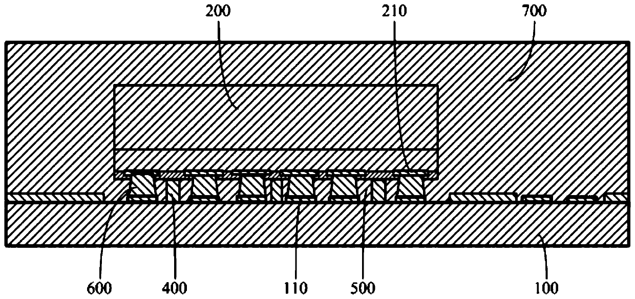
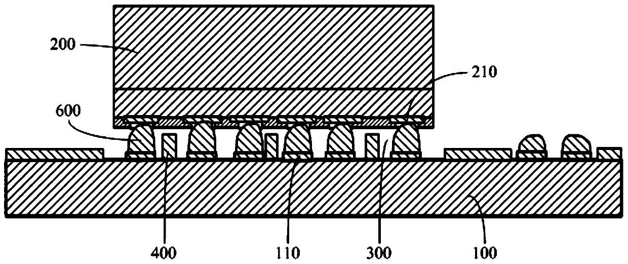
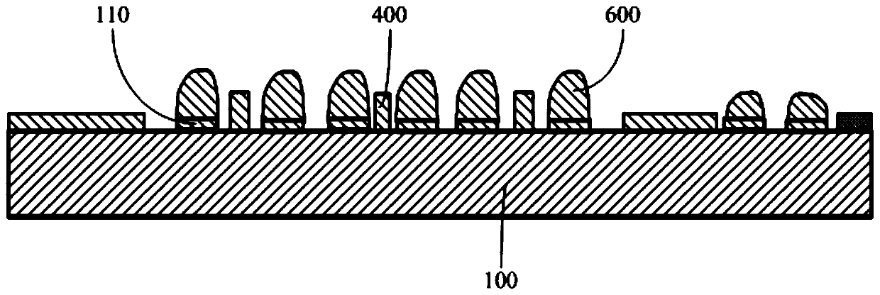
[0042] Please refer to Figure 1 to Figure 13 , the embodiment of the present invention discloses a circuit board device, and the disclosed circuit board device includes a substrate 100 , a chi...


PUM


Abstract

The invention discloses a circuit board device, and the circuit board device comprises: a substrate (100) which is provided with a first bonding pad (110); a chip module (200) wich is provided with asecond bonding pad (210), wherein the first bonding pad (110) is electrically connected with the second bonding pad (210), and a filling space (300) is formed between the chip module (200) and the substrate (100); a supporting piece (400) which is supported between the substrate (100) and the chip module (200); and a filling part (500) which is filled into the filling space (300) . According to the scheme, the problem that the packaged chip is prone to short circuit in the packaging process on the circuit board can be solved. The invention further discloses a preparation method of the circuitboard device and electronic equipment.

Description

technical field [0001] The invention relates to the technical field of circuit boards, in particular to a circuit board device, a preparation method thereof, and electronic equipment. Background technique [0002] At present, chips generally have WLCSP (Wafer Level Chip Scale Packaging) packaged chips according to the package type, BGA (Ball Grid Array Package, ball grid array package) packaged chips, LGA (Land Grid Array, grid array package) Package) packaged chips and QFN (Quad Flat No-lead-Package, square flat no-lead package) packaged chips, etc., in which the upper layer of the packaging structure of the LGA packaged chip is a plastic packaging material, and the lower layer is a packaged carrier board, but the LGA packaged chip There is only a pad at the bottom, and solder paste needs to be printed on the circuit board for soldering when soldering at the board level. [0003] In the specific board-level soldering process, when the LGA package chip is mounted on the cir...

Claims


Application Information

Patent Timeline
Patent Type & Authority Applications(China)
IPC IPC(8): H01L23/492H01L23/488H01L23/12H01L23/13H01L23/31
CPCH01L23/492H01L23/488H01L23/12H01L23/13H01L23/3121H01L2224/13H01L2224/1354H01L2224/81192H01L2224/8114H01L2224/16225H01L2924/181H01L2924/00012
Inventor 杨望来
Owner 维沃移动通信(重庆)有限公司
Why Eureka
Try Eureka