Semiconductor structure and process thereof

a technology of semiconductors and semiconductors, applied in semiconductor devices, semiconductor/solid-state device details, electrical devices, etc., can solve the problems of inferior performance, reduced gate capacitance, and conventional poly-silicon gate faces, so as to reduce the height of metal gates, reduce the loading effect of polishing processes, and avoid void generation

Active Publication Date: 2016-10-13
MARLIN SEMICON LTD
View PDF5 Cites 12 Cited by
  • Summary
  • Abstract
  • Description
  • Claims
  • Application Information

AI Technical Summary

Benefits of technology

[0010]According to the above, the present invention provides a semiconductor structure and process thereof, which sequentially forms a metal gate strip and a cap layer, and then cuts off the cap layer and the metal gate strip to form an isolation slot therein. Thereby, the present invention can have advantages rather than a conventional method of forming an isolation slot in a sacrificial gate strip before forming metal gates. For example, advantages include avoiding residues of sacrificial gate materials being left in a trench for forming the isolation slot, reducing shorter heights of metal gates occurring caused by loss of a dielectric layer, avoiding voids generating by gap filling difficulty of metal gate materials beside the isolation slot, reducing loading effect of polishing processes, reducing the etching of a height of a trench for forming the isolation slot, and solving problems of over-losing metal gates and enlarging critical dimension (CD). Therefore, the present invention can improve many problems occurring during processes, and thus enhance size miniaturization of a formed semiconductor component and improve the reliability and yields of the formed semiconductor component.

Problems solved by technology

With the trend towards scaling down the size of semiconductor devices, however, conventional poly-silicon gates face problems such as inferior performance due to boron penetration and unavoidable depletion effect.
This increases equivalent thickness of the gate dielectric layer, reduces gate capacitance, and worsens a driving force of the devices.

Method used


Image

  • Semiconductor structure and process thereof
  • Semiconductor structure and process thereof
  • Semiconductor structure and process thereof

Examples


Embodiment Construction

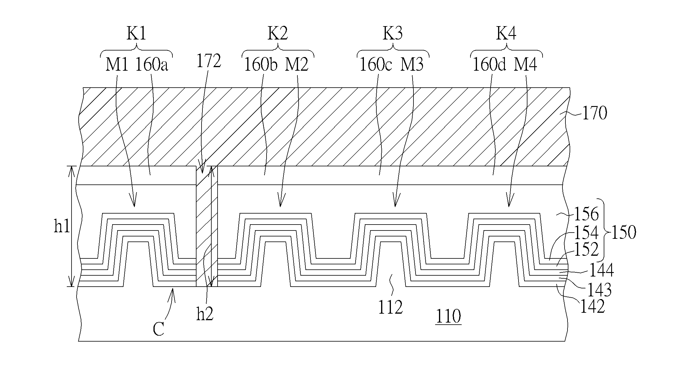
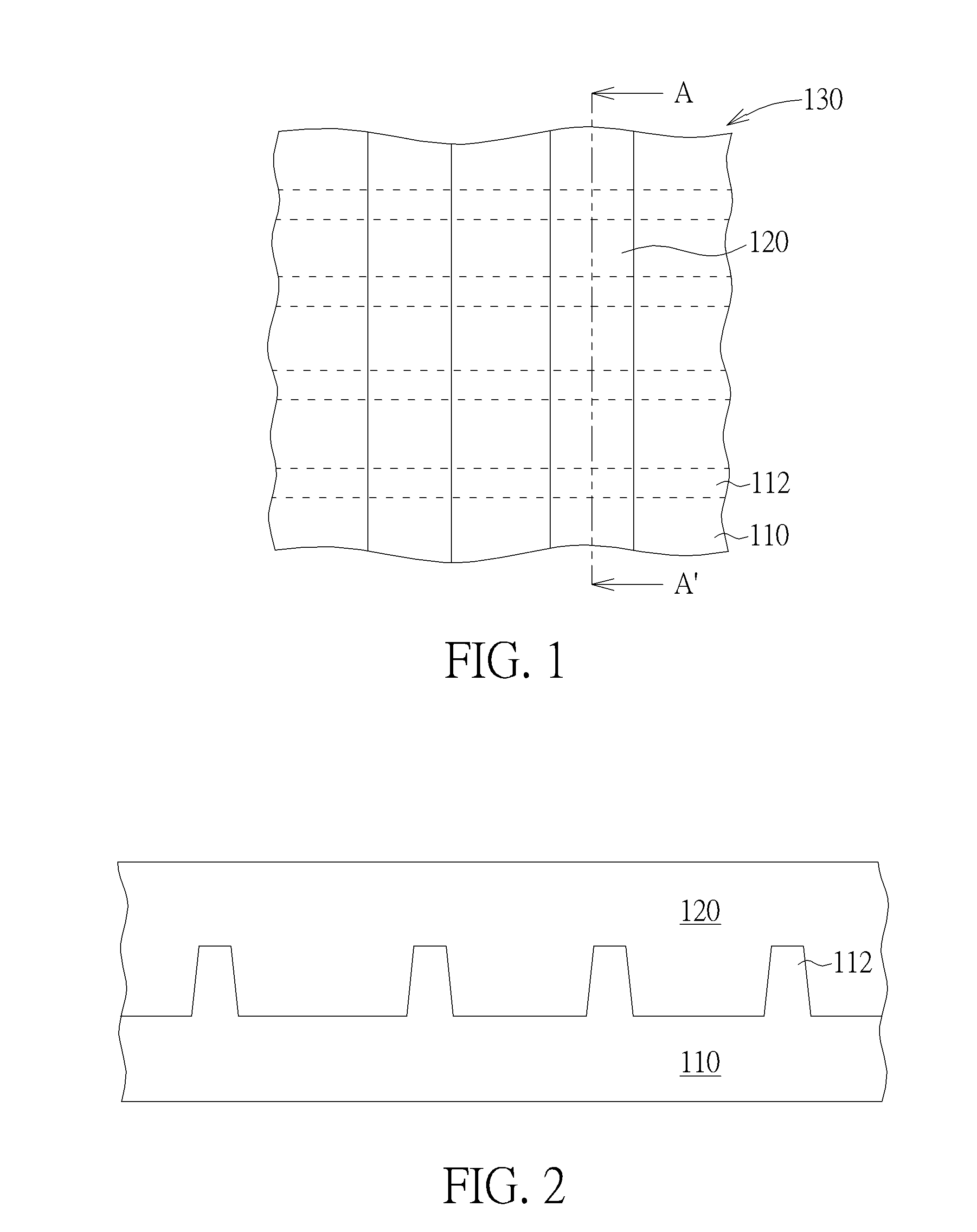
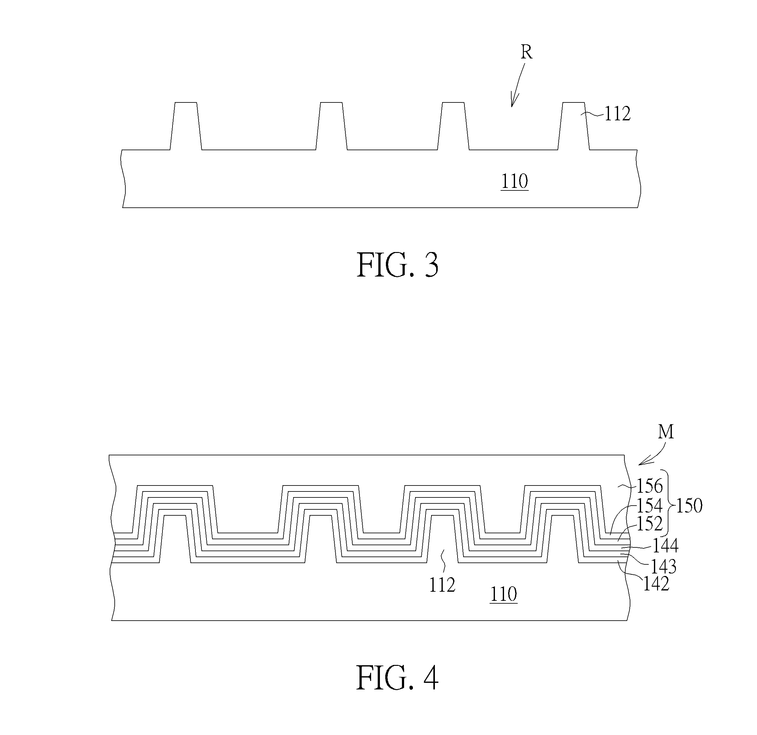
[0015]FIG. 1 schematically depicts a top view of a semiconductor process according to an embodiment of the present invention. As shown in FIG. 1, a plurality of fin structures 112 are formed in a substrate 110. The method of forming the fin structures 112 may include, but is not limited to, the following. A bulk bottom substrate (not shown) is provided. A hard mask layer (not shown) is formed on the bulk bottom substrate (not shown) and is patterned to define the locations of the fin structures 112, which will be formed in the bulk bottom substrate (not shown). An etching process is performed to form the fin structures 112 in the bulk bottom substrate (not shown), and then isolation structures (not shown) may be formed between bottom parts of the fin structures 112. Thus, the fin structures 112 located in the substrate 110 are formed completely. In one embodiment, the hard mask layer (not shown) is removed after the fin structures 112 are formed, and a tri-gate MOSFET can be formed ...


PUM


Abstract

A semiconductor process includes the following step. A metal gate strip and a cap layer are sequentially formed in a trench of a dielectric layer. The cap layer and the metal gate strip are cut off to form a plurality of caps on a plurality of metal gates, and a gap isolates adjacent caps and adjacent metal gates. An isolation material fills in the gap. The present invention also provides semiconductor structures formed by said semiconductor process. For example, the semiconductor structure includes a plurality of stacked structures in a trench of a dielectric layer, where each of the stacked structures includes a metal gate and a cap on the metal gate, where an isolation slot isolates and contacts adjacent stacked structures at end to end, and the isolation slot has same level as the stacked structures.

Description

BACKGROUND OF THE INVENTION[0001]1. Field of the Invention[0002]The present invention relates generally to a semiconductor structure and process thereof, and more specifically to a semiconductor structure applying isolation slots in metal gate strips and process thereof.[0003]2. Description of the Prior Art[0004]Poly-silicon is conventionally used as a gate electrode in semiconductor devices, such as the metal-oxide-semiconductor (MOS). With the trend towards scaling down the size of semiconductor devices, however, conventional poly-silicon gates face problems such as inferior performance due to boron penetration and unavoidable depletion effect. This increases equivalent thickness of the gate dielectric layer, reduces gate capacitance, and worsens a driving force of the devices. Therefore, work function metals that are suitable for use as the high-K gate dielectric layer are used to replace the conventional poly-silicon gate to be the control electrode.[0005]As work function metals...

Claims


Application Information

Patent Timeline
Patent Type & Authority Applications(United States)
IPC IPC(8): H01L21/762H01L21/02H01L29/423H01L21/768
CPCH01L21/76224H01L21/76897H01L29/4236H01L21/7684H01L21/02274H01L21/823431H01L21/845H01L29/401H01L23/535H01L29/0649H01L29/42384
Inventor GAN, TIAN CHOYHSIAO, CHU-YUNHUANG, CHUN-CHEHSU, CHIA-FU
Owner MARLIN SEMICON LTD
Why Eureka
Try Eureka