
Preparation method of shallow trench isolation structure
A technology of isolation structure and shallow trench, which is applied in the field of preparation of shallow trench isolation structure, can solve problems such as critical dimension reduction, affecting device performance, and affecting device saturation current, so as to avoid void or gap defects, reduce critical dimension, The effect of reducing consumption
- Summary
- Abstract
- Description
- Claims
- Application Information
AI Technical Summary
Problems solved by technology
Method used
Image

Examples
Embodiment Construction
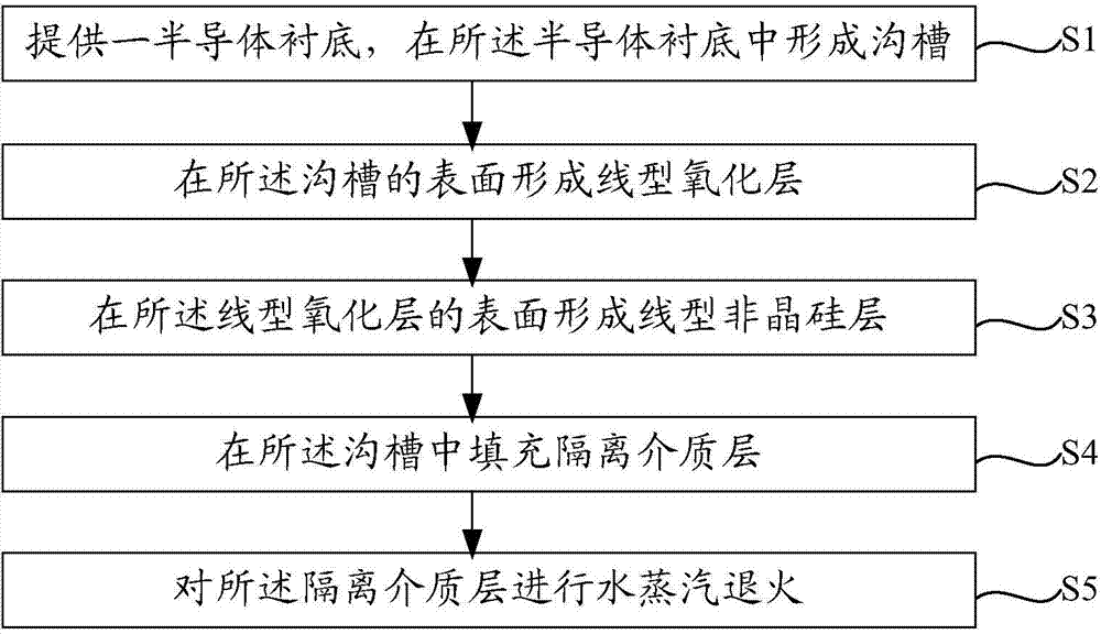
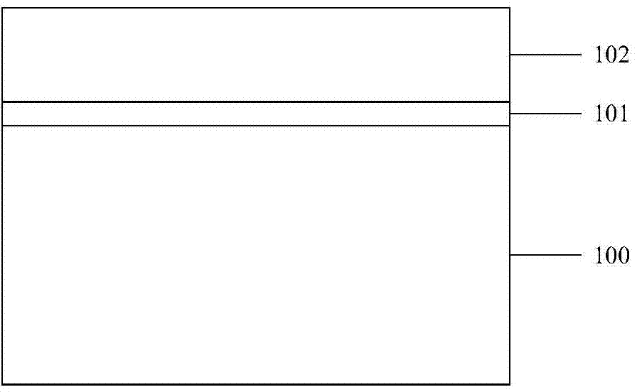
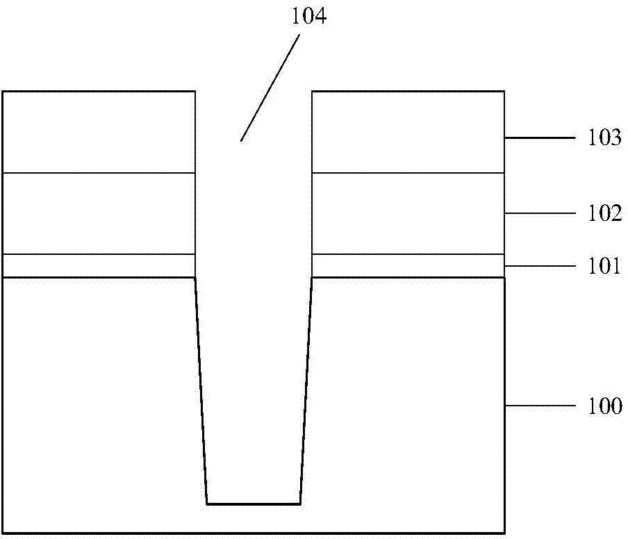
[0031] In order to make the purpose and features of the present invention more obvious and understandable, the specific implementation of the present invention will be further described below in conjunction with the accompanying drawings. However, the present invention can be implemented in different forms and should not be limited to the described embodiments. The following will be combined with figure 1 and Figures 2A to 2F The preparation method of the shallow trench isolation structure is further described in detail with specific embodiments. in, Figure 2A It is a schematic cross-sectional view of the device structure after silicon nitride is deposited on the active region of the semiconductor substrate, Figure 2B It is a schematic cross-sectional view of the device structure after trench etching in the semiconductor substrate, Figure 2C It is a schematic cross-sectional view of the device structure after the silicon nitride post-pull process, Figure 2D It is a sc...
PUM
 Abstract
Description
Claims
Application Information