A low on-resistance trench mosfet structure and its preparation method

A low on-resistance, trench-type technology, used in semiconductor/solid-state device manufacturing, circuits, electrical components, etc., can solve problems such as non-uniform distribution of potential, and achieve uniform distribution, reduced on-resistance, and large divergence angle. Effect

Active Publication Date: 2020-11-17
江苏长晶科技股份有限公司
View PDF4 Cites 0 Cited by
  • Summary
  • Abstract
  • Description
  • Claims
  • Application Information

AI Technical Summary

Problems solved by technology

[0004] The purpose of the present invention is to solve the shortcoming of non-uniform potential distribution near the bottom area of ​​the trench in the prior art, and propose a low on-resistance trench MOSFET structure and its preparation method

Method used


Image

  • A low on-resistance trench mosfet structure and its preparation method
  • A low on-resistance trench mosfet structure and its preparation method
  • A low on-resistance trench mosfet structure and its preparation method

Examples


Embodiment Construction

[0033] Below in conjunction with specific embodiment, further illustrate the present invention. These examples are only for illustrating the present invention and are not intended to limit the scope of the present invention. In the description of the present invention, it should be noted that unless otherwise specified and limited, the terms "installation", "installation" and "connection" should be interpreted in a broad sense, for example, it can be a fixed connection or an optional connection. Detachable connection, or integral connection; it can be mechanical connection or electrical connection; it can be direct connection or indirect connection through an intermediary, and it can be the internal communication of two components. Those of ordinary skill in the art can understand the specific meanings of the above terms in the present invention in specific situations.

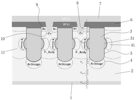
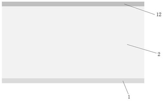
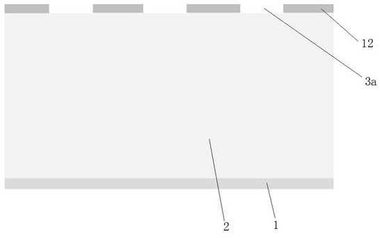
[0034] Now in conjunction with the accompanying drawings, the structural features of the present invention...


PUM


Abstract

The invention discloses a low-on-resistance groove type MOSFET structure and a preparation method thereof. The invention relates to the semiconductor technology. The low-on-resistance trench type MOSFET structure comprises a semiconductor substrate and also comprises a semiconductor epitaxial layer main body, a diaphragm layer and a metal covering layer are sequentially fixed on the semiconductorsubstrate, grooves which are arranged tightly and are of small channel structures are formed in the semiconductor epitaxial layer main body and located on a lower portion of the diaphragm layer in anarray mode, at least one annular groove is formed in each groove in the length direction of the groove, and the grooves and the annular grooves are filled with polycrystalline silicon. The bottoms ofthe grooves and the outer sides of the annular grooves are respectively provided with first ion distribution regions and second ion distribution regions of which the ion concentration is higher than that of the semiconductor epitaxial layer main body. The invention further provides the preparation method of the low-on-resistance trench MOSFET structure, the distribution of current in the whole epitaxial layer is more uniform, and the divergence angle is larger such that the on-resistance of the device is reduced, and the overall breakdown voltage of the device is improved.

Description

technical field [0001] The invention belongs to semiconductor technology, and in particular relates to a low conduction resistance trench MOSFET structure and a preparation method thereof. Background technique [0002] With the rapid development of power semiconductor devices represented by power MOSFET devices, power semiconductor devices are now widely used in computer, traffic, consumer electronics, automotive electronics and other industries. Reasonable management requires effective control of the application of voltage and current, and these controls are inseparable from power devices. [0003] In the ordinary trench MOSFET structure, the current flowing out of the channel region expands to the drain region at a divergence angle of approximately 45° after entering the epitaxial body region. The distribution of the current in the entire epitaxial layer is not uniform, and the divergence angle is limited. The on-resistance of the device is increased, and the potential di...

Claims


Application Information

Patent Timeline
Patent Type & Authority Patents(China)
IPC IPC(8): H01L27/088H01L29/06H01L29/36H01L29/423H01L21/8234
CPCH01L21/8234H01L27/088H01L29/0607H01L29/0684H01L29/36H01L29/4236
Inventor 杨国江赖信彰于世珩
Owner 江苏长晶科技股份有限公司
Why Eureka
Try Eureka