Printed wiring board device

A technology for printed circuit boards and substrates, applied in the directions of printed circuits, printed circuits, circuit devices, etc., can solve the problems of high manufacturing price and difficult application, and achieve the effect of suppressing electromagnetic radiation

Inactive Publication Date: 2003-07-02
FUJIFILM BUSINESS INNOVATION CORP
View PDF0 Cites 3 Cited by
  • Summary
  • Abstract
  • Description
  • Claims
  • Application Information

AI Technical Summary

Problems solved by technology

[0008] However, the Figure 19 The past method shown has the disadvantages of forming two ground planes 32A, 32B, connecting a resistor 33 between them, changing the dielectric constant of the dielectric 34A, 34B between the power supply plane 31 and the ground planes 32A, 32B, etc. , for a general printed circuit board, the structure of the printed circuit board itself must be greatly changed. At the same time, due to the difference in size and shape of the printed circuit board, matching conditions for suppressing electromagnetic radiation must be set for each printed circuit board, Therefore, it is quite difficult to apply to actual products. Even if it can be applied, its manufacturing price is also very high

Method used


Image

  • Printed wiring board device
  • Printed wiring board device
  • Printed wiring board device

Examples


Embodiment Construction

[0056] Referring to the accompanying drawings, the detailed description is the best embodiment for implementing the present invention.

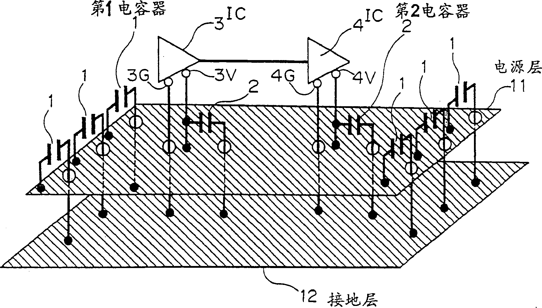
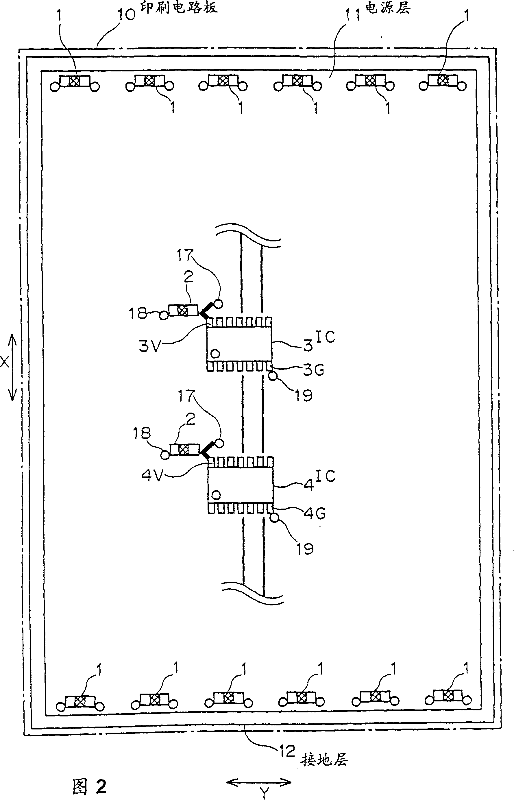
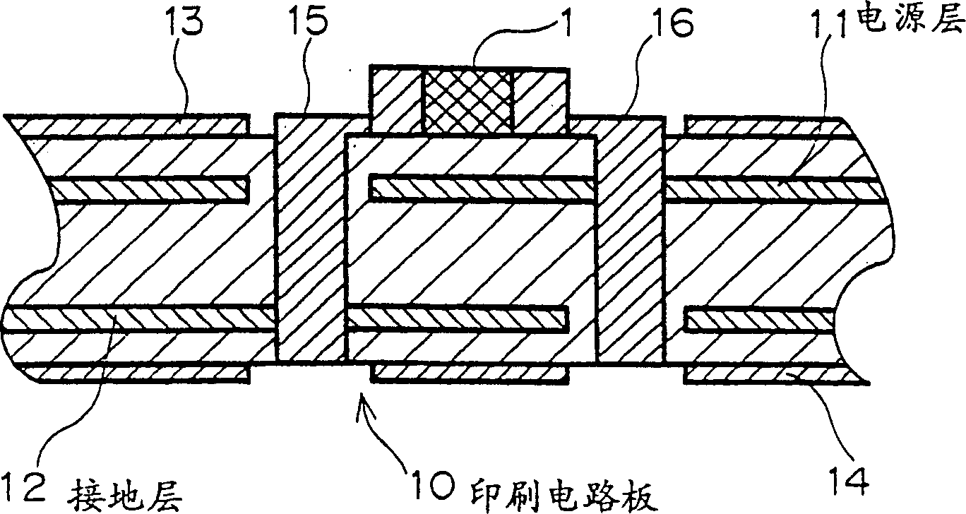
[0057] figure 1 ~ Fig. 4 shows an example of the printed circuit board device of the present invention. figure 1 The schematic composition of the device is given, and Fig. 2 is a schematic plan view of the device, image 3 Showing the cross-sectional configuration of the configuration portion of the first capacitor, FIG. 4 is a schematic plan view of a digital integrated circuit as an active element and a configuration portion of the second capacitor.

[0058] The printed circuit board 10 of the printed circuit board device of this example is as image 3 Shown is a 4-layer printed circuit board having a power layer 11 , a ground layer 12 , a graphics layer 13 and a graphics layer 14 . It is also acceptable to have one or more graphic layers between the power supply layer 11 and the ground layer 12 .

[0059] In addition, the printed cir...


PUM


Abstract

A printed wiring board device used for electronic equipment, such as the information equipment, etc. A printed wiring board (10) has a power source layer (11) and a ground layer (12) and is mounted with active elements (3 and 4), such as digital ICs, etc. A first capacitor (1) which conductively couples the layers (11 and 12) with each other at a high frequency is provided in the peripheral section of one end side or the other end side of the section of the board (10) where the layers (11 and 12) are faced to each other. Second capacitors (2) which respectively supply transient currents to the active elements (3 and 4) are provided between the power supply pins (3V and 4V) of the elements (3 and 4) and the ground layer (12) near the elements (3 and 4). Therefore, the electromagnetic radiation caused by the power source layer (11) and the ground layer (12) of the printed wiring board (10) can be suppressed easily and remarkably.

Description

field of invention [0001] The present invention relates to a printed circuit board device for electronic equipment such as information equipment, and electronic equipment such as information equipment to which the printed circuit board is applied. Background technique [0002] In recent years, interference radiation of electromagnetic waves has become a problem in various information devices. Moreover, since the electromagnetic radiation mainly has a spectrum corresponding to the higher harmonics of the clock pulse on the printed circuit board, it has been considered so far that the electromagnetic radiation is mainly caused by the clock pulse signal or the signal of a digital signal synchronized with it. Therefore, various electromagnetic wave radiation prevention measures are taken for the signal lines on the printed circuit board and the wiring harnesses connected to them. [0003] Specifically, consider the following three points; (1) perform low-pass filter processing ...

Claims


Application Information

Patent Timeline
Patent Type & Authority Patents(China)
IPC IPC(8): H05K1/02
CPCH05K1/023H05K1/0231H05K2201/10022H05K2201/09309H05K2201/10522H05K2201/10636H05K2201/10446H05K2201/10689Y02P70/50H05K1/02
Inventor 井口大介上野修
Owner FUJIFILM BUSINESS INNOVATION CORP
Why Eureka
Try Eureka