Pixel unit, pixel array and liquid crystal panel thereof

A technology of pixel unit and pixel array, which is applied in the direction of instruments, nonlinear optics, optics, etc., and can solve the problems of low charge release ability and prone to afterimages

Active Publication Date: 2020-07-07
XIANYANG CAIHONG OPTOELECTRONICS TECH CO LTD
View PDF12 Cites 1 Cited by
  • Summary
  • Abstract
  • Description
  • Claims
  • Application Information

AI Technical Summary

Problems solved by technology

Furthermore, the sub-pixel is affected by the potential of the ITO floatin...

Method used


Image

  • Pixel unit, pixel array and liquid crystal panel thereof
  • Pixel unit, pixel array and liquid crystal panel thereof
  • Pixel unit, pixel array and liquid crystal panel thereof

Examples


Embodiment Construction

[0041] In the following description, many technical details are proposed in order to enable readers to better understand the application. However, those skilled in the art can understand that the technical solutions claimed in this application can be realized even without these technical details and various changes and modifications based on the following implementation modes.

[0042] In order to make the object, technical solution and advantages of the present invention clearer, the present invention will be described in further detail below in conjunction with specific examples, but the implementation of the present invention is not limited thereto.

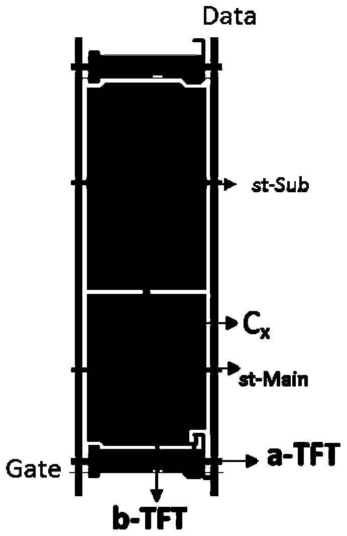
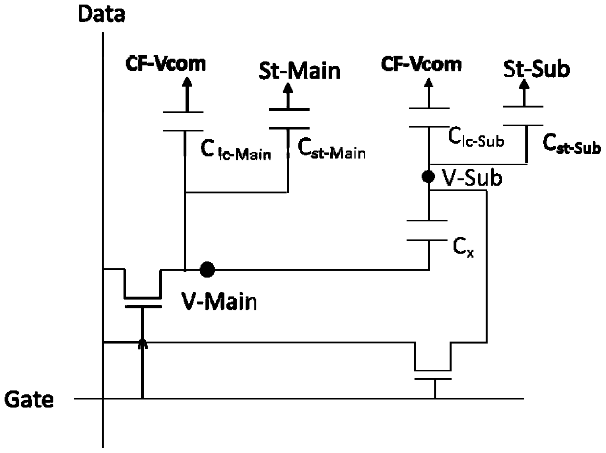
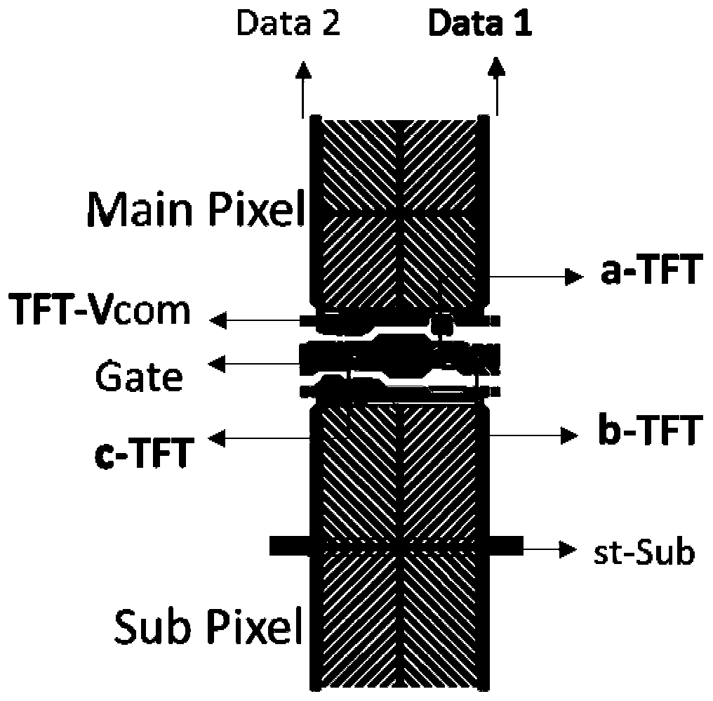
[0043] Such as Figure 3-Figure 4 as shown, image 3 A schematic structural diagram of a pixel array provided by an embodiment of the present invention; Figure 4 A schematic diagram of a driving circuit provided for an embodiment of the present invention; the pixel array of this embodiment includes a plurality of scanning l...


PUM


Abstract

The invention relates to a pixel unit, a pixel array and a liquid crystal panel thereof; each pixel unit comprises a first switch, a second switch and a third switch; the first switch and the second switch are electrically connected with the same data line and the same scanning line, the third switch is connected with the second switch in parallel, and the third switch is electrically connected with the same scanning line; the main pixel electrode is electrically connected with the first switch; the sub-pixel electrode is electrically connected with the second switch and the third switch; thecoupling electrode is electrically connected with the second switch and the third switch; and the third switch is also electrically connected with the common line. By adding the third switch and connecting the third switch and the second switch in parallel, the charge and discharge speed of the second storage capacitor is increased, the charge release capacity of the second storage capacitor is enhanced, and residual images can be improved.

Description

technical field [0001] The invention relates to the field of liquid crystal display screens, in particular to a pixel unit, a pixel array and a liquid crystal panel thereof. Background technique [0002] Liquid Crystal Display (LCD) has many advantages such as thin body, power saving, and no radiation, and has been widely used, such as: LCD TV, mobile phone, personal digital assistant (PDA), digital camera, computer screen or Laptop screens, etc., dominate the field of flat panel displays. [0003] The current mainstream liquid crystal display panel is composed of a thin film transistor array substrate (Thin Film TransistorArray Substrate, TFT Array Substrate) and a color filter (Color Filter, CF) substrate, and between the TFT substrate and the CF substrate Fill the liquid crystal. The direction of the liquid crystal molecules is controlled by electrification or not, and the light from the backlight module is refracted to produce a picture. [0004] Among them, one side ...

Claims


Application Information

Patent Timeline
IPC IPC(8): G02F1/1362G02F1/1343
CPCG02F1/1362G02F1/136213G02F1/136286G02F1/134309
Inventor 胡佳乔吴永良陈宥烨
Owner XIANYANG CAIHONG OPTOELECTRONICS TECH CO LTD
Why Eureka
Try Eureka