Solid-state imaging device, method for driving solid-state imaging device, and electronic apparatus

A camera device, solid-state technology, applied in the direction of TV, circuit, color TV, etc., can solve the problem of unable to read the global shutter and so on

Active Publication Date: 2020-07-07
普里露尼库斯新加坡私人有限公司
View PDF14 Cites 1 Cited by
  • Summary
  • Abstract
  • Description
  • Claims
  • Application Information

AI Technical Summary

Problems solved by technology

[0011] However, this type of CMOS image sensor can transmit signals at high speed, but has the disadvantage of not being able to read the global shutter (global shutter)

Method used


Image

  • Solid-state imaging device, method for driving solid-state imaging device, and electronic apparatus
  • Solid-state imaging device, method for driving solid-state imaging device, and electronic apparatus
  • Solid-state imaging device, method for driving solid-state imaging device, and electronic apparatus

Examples


no. 1 approach

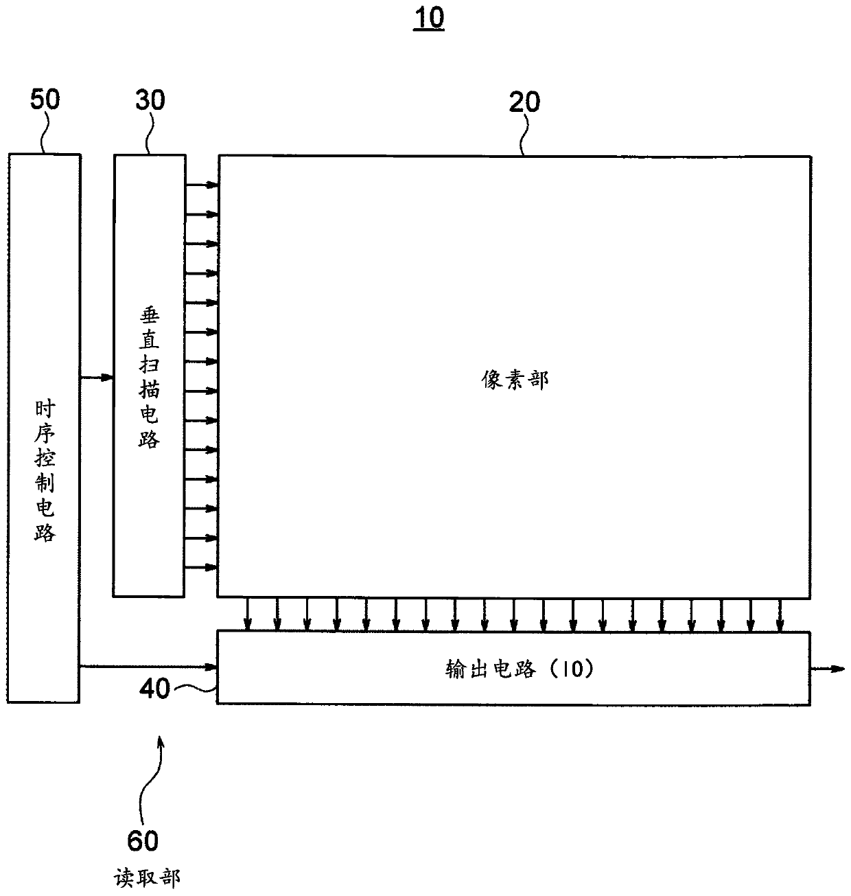
[0073] figure 1 It is a block diagram showing a configuration example of the solid-state imaging device according to the first embodiment of the present invention.

[0074] In the present embodiment, the solid-state imaging device 10 is constituted by, for example, a CMOS image sensor including digital pixels as pixels.

[0075] like figure 1 As shown, the solid-state imaging device 10 includes a pixel unit 20 as an imaging unit, a vertical scanning circuit (row scanning circuit) 30, an output circuit 40, and a timing control circuit 50 as main components.

[0076] The reading section 60 of the pixel signal is constituted by, for example, the vertical scanning circuit 30 , the output circuit 40 , and the timing control circuit 50 among these components.

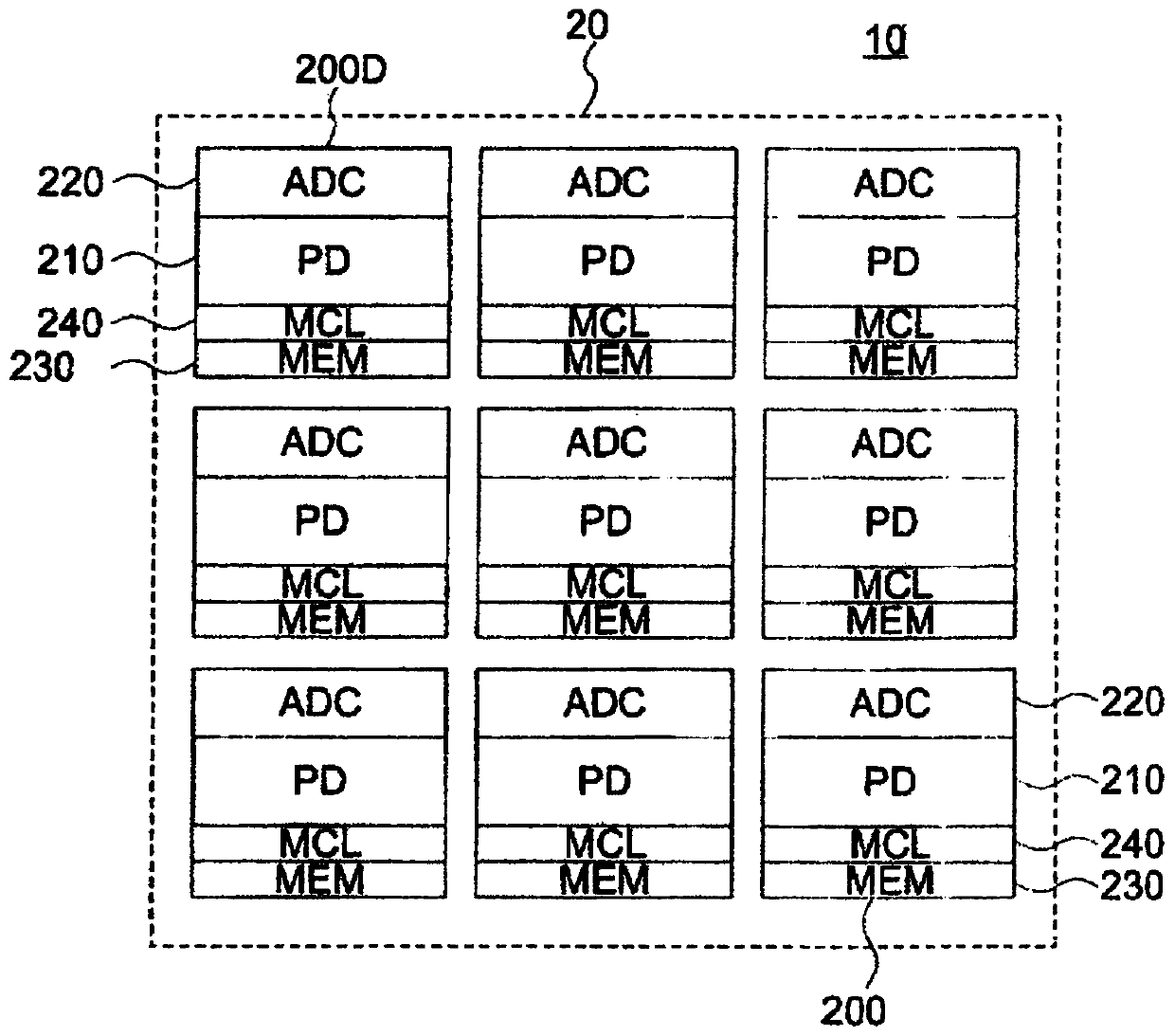
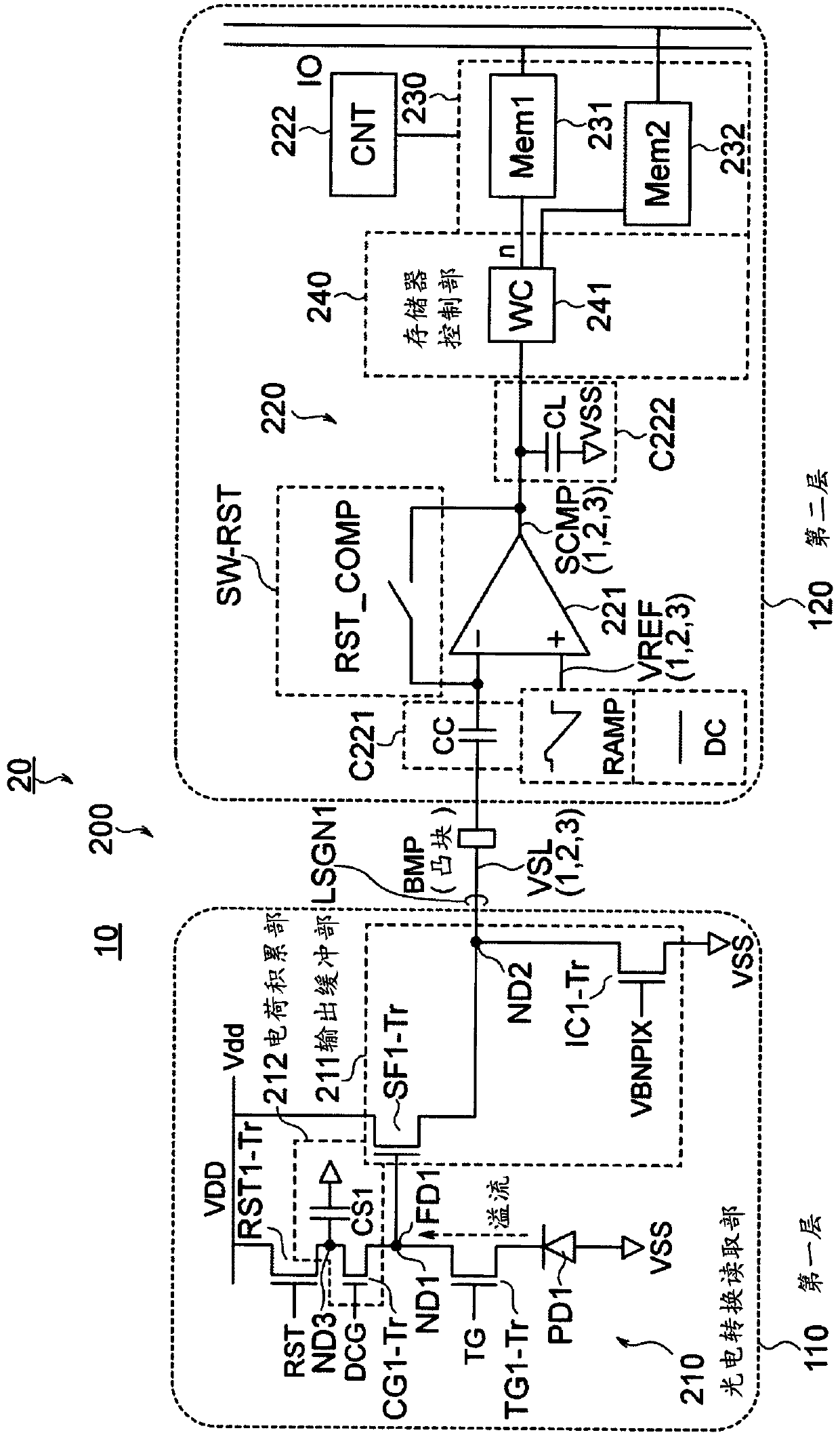
[0077] In the first embodiment, the solid-state imaging device 10 includes a photoelectric conversion reading unit, an AD (analog-to-digital) conversion unit, and a memory unit as digital pixels in the pixel unit 20, and is...

no. 2 approach

[0388] Figure 30 This is a diagram for explaining the solid-state imaging device according to the second embodiment of the present invention, and is a diagram showing an example of selection processing between the time stamp ADC mode operation and the linear ADC mode operation.

[0389] The solid-state imaging device 10A of the second embodiment differs from the solid-state imaging device 10 of the first embodiment in the following points.

[0390] In the solid-state imaging device 10 of the first embodiment, the time stamp (TS) ADC mode operation and the linear (Lin) ADC mode operation are continuously performed.

[0391] On the other hand, in the solid-state imaging device 10A according to the second embodiment, the time stamp (TS) ADC mode operation and the linear (Lin) ADC mode operation can be selectively performed according to the illuminance.

[0392] exist Figure 21 In the case of the normal illuminance ( ST51 ), the time stamp ADC mode operation and the linear ADC...

no. 3 approach

[0397] Figure 31 It is a figure which shows the structural example of the pixel of the solid-state imaging device concerning 3rd Embodiment of this invention.

[0398] The solid-state imaging device 10B of the third embodiment is different from the solid-state imaging device 10 of the first embodiment in the following points.

[0399] In the solid-state imaging device 10B according to the third embodiment, the current transistor IC1 -Tr serving as the current source is not arranged on the first substrate 110 side, but is arranged, for example, at the input of the AD conversion unit 220 on the second substrate 120 side. side.

[0400] According to the third embodiment, the same effects as those of the first embodiment can be obtained.

[0401] The solid-state imaging devices 10 , 10A, and 10B described above can be applied to electronic devices such as digital cameras, video cameras, portable terminals, monitoring cameras, and medical endoscope cameras as imaging devices.

...


PUM


Abstract

Provided is a solid-state imaging device, a method for driving solid-state imaging device, and an electronic apparatus, by which large dynamic range, high frame rate, and high effective access of a memory can be essentically achieved. A comparator (221) is configured to perform a first comparing operation of outputting a digital first comparison result signal obtained by processing the overflow charges overflowing from PD1 to FD1 in the storing period, a second comparing operation of outputting a digital second comparison result signal obtained by processing the charges stored in PD1 that aretransferred to FD1 in the transfer period, and a third comparing operation of outputting a digital third comparison result signal obtained by processing the charges stored in PD1 that are transferredto FD1 in the transfer period and the charges stored in the charge storing part, and a memory control part (240) controls whether or not to allow writing of the data corresponding to the third comparison result signal into a memory part (230), depending on the states of the first and second comparison result signals.

Description

technical field [0001] The present invention relates to a solid-state imaging device, a driving method of the solid-state imaging device, and electronic equipment. Background technique [0002] Complementary Metal Oxide Semiconductor (CMOS) image sensors have been put into practical use as solid-state imaging devices (image sensors) using photoelectric conversion elements that detect light and generate electric charges. [0003] CMOS image sensors are widely used as part of various electronic devices such as digital cameras, video cameras, surveillance cameras, medical endoscopes, personal computers (PCs), and portable terminal devices (mobile devices) such as mobile phones. [0004] The CMOS image sensor has an FD amplifier including a photodiode (photoelectric conversion element) and a floating diffusion layer (FD: Floating Diffusion) in each pixel. The mainstream reading type of the CMOS image sensor is column parallel output. type, that is, select a row in the pixel arr...

Claims


Application Information

Patent Timeline
Patent Type & Authority Applications(China)
IPC IPC(8): H04N5/374H04N5/3745H04N5/378
CPCH04N25/77H04N25/76H04N25/75H04N25/59H04N25/772H04N25/79H01L27/14612H01L27/14638H01L27/14643
Inventor 盛一也大高俊德高柳功
Owner 普里露尼库斯新加坡私人有限公司
Why Eureka
Try Eureka