

Double-layer circuit and manufacturing method thereof
A manufacturing method and circuit technology, applied in multilayer circuit manufacturing, printed circuit manufacturing, printed circuit, etc., can solve the problems of low production efficiency of liquid metal double-layer circuits
- Summary
- Abstract
- Description
- Claims
- Application Information
AI Technical Summary
Problems solved by technology
Method used
Image

Examples
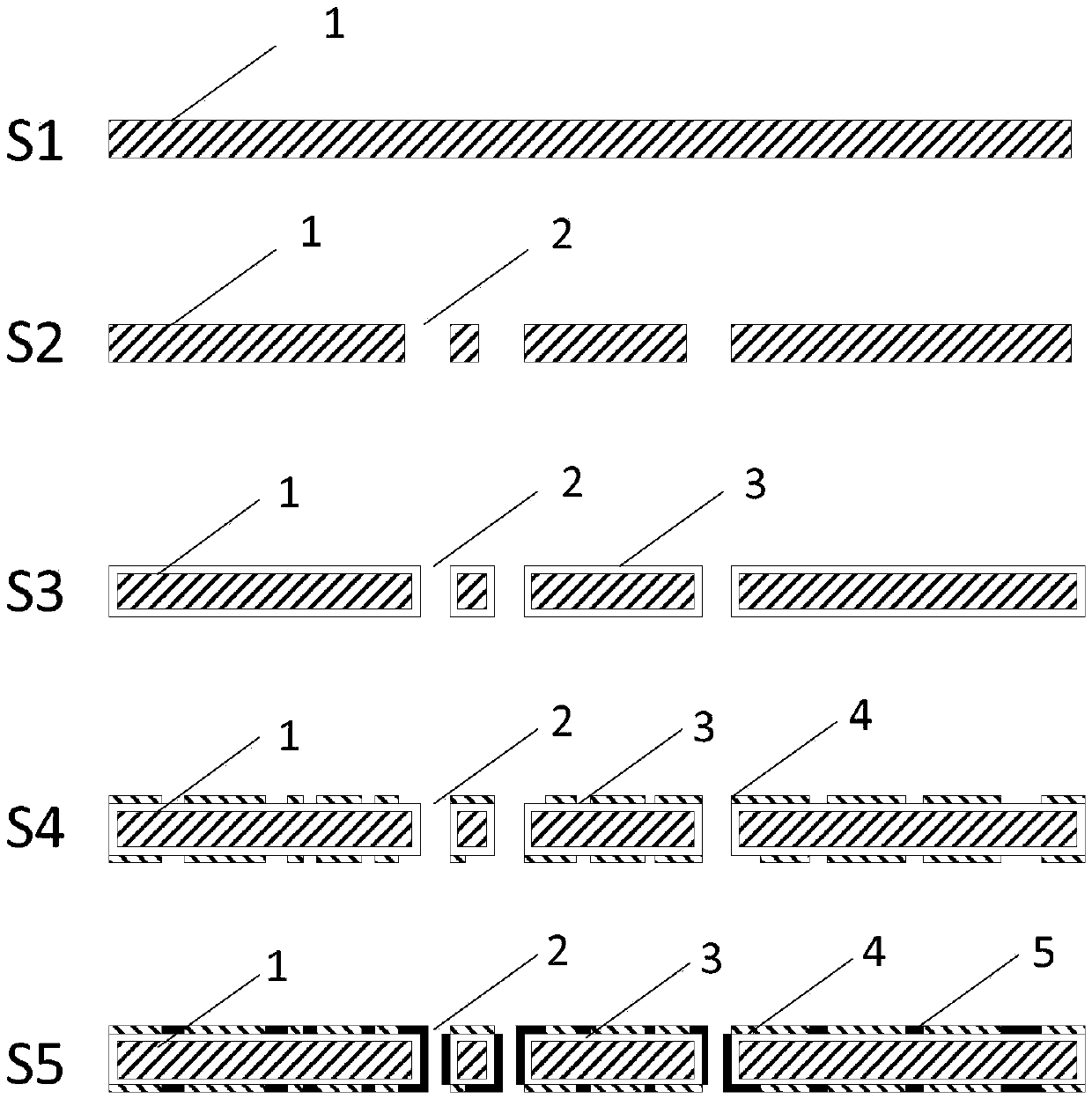
Embodiment approach 1
[0042] Step a, select PET film as the base material, the thickness of the base material is 200 μm;
[0043] Step b, drilling required via holes on the base material;
[0044] Step c, performing surface treatment on the base material, cleaning both sides of the base material and the inner wall of the via hole;
[0045] Step d, immersing the base material in the polyurethane colloid for 15 seconds, drying and curing after taking it out, forming a surface modification layer of 50 μm on the surface of the base material;
[0046] Step e, forming a solder resist layer on the surface modification layer on both sides of the base material by laser printing toner; wherein, the solder resist layer includes a silk screen layer of the circuit;
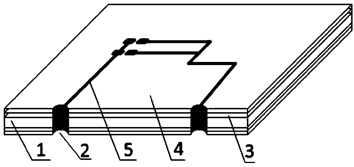
[0047] Step f, put the substrate into the liquid metal coating device and use the roller set to coat the liquid metal on both sides of the substrate; wherein, the liquid metal on the inner wall of the via hole is squeezed into the via hole by the ...
PUM
| Property | Measurement | Unit |
|---|---|---|
| Thickness | aaaaa | aaaaa |
| Thickness | aaaaa | aaaaa |
| Thickness | aaaaa | aaaaa |
Abstract
Description
Claims
Application Information