Trench gate MOS power device and gate manufacturing method thereof
A manufacturing method and technology of power devices, which are applied in semiconductor/solid-state device manufacturing, semiconductor devices, electrical components, etc., can solve problems affecting the long-term reliability of gate devices, difficult to control switching behavior, and difficult to reduce switching losses, etc., to achieve a solution The switching behavior is difficult to control, the ability to withstand carrier bombardment is strong, and the effect of reducing switching loss
- Summary
- Abstract
- Description
- Claims
- Application Information
AI Technical Summary
Problems solved by technology
Method used
Image

Examples
Embodiment 1
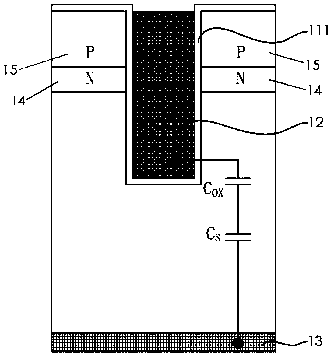
[0047] like figure 2 As shown, this embodiment provides a trench gate MOS power device, taking a trench gate IGBT (InsulatedGate Bipolar Transistor) as an example, which includes a channel region. Specifically, the channel region of the trench gate IGBT in this embodiment is The region is the P-well region 15 . Usually, in order to form a complete trench gate IGBT structure, an N+ source region (not shown) in contact with the emitter electrode is also provided above the P well region 15 , which is common knowledge and will not be discussed in detail.
[0048] In this embodiment, a carrier injection region adjacent to the P well region 15 is further provided below the P well region 15 . Specifically, the carrier injection region in this embodiment is the N well region 14 and the N well region. 14 When the trench gate IGBT is operating, the level of carrier injection can be improved. The gate oxide layers corresponding to the P-well region 15 and the N-well region 14 are the ...
Embodiment 2
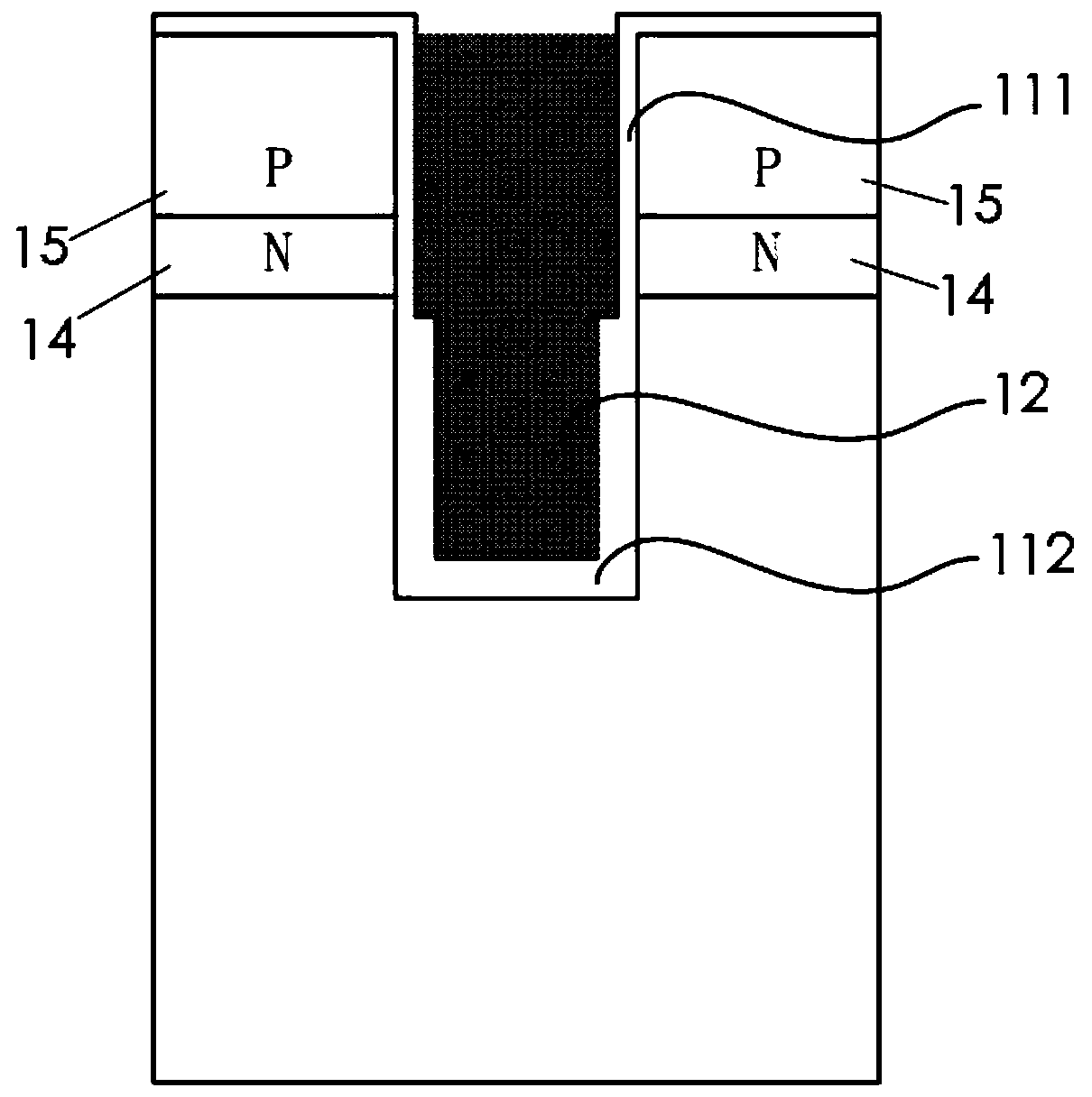
[0064] The N-well region 14 only serves to improve the level of carrier injection, and the removal of the N-well region 14 does not affect the basic function of the trench gate IGBT. The trench gate IGBT provided by this embodiment does not have a carrier injection region, that is, the N well region 14 is removed. When fabricating the gate of the trench gate IGBT device, the N well region 14 is no longer formed in step S1, and the bottom surface of the trench 16 is lower than the bottom surface of the P well region 15; in step S302, the exposed photoresist 171 The bottom surface of the P-well region 15 is located near the bottom surface of the P-well region 15 , and may be slightly higher or lower or flush with the bottom surface of the P-well region 15 . In step S304 , the upper surface of the finally etched thick oxide layer 112 is slightly lower than the bottom surface of the P well region 15 . The rest are the same as the first embodiment.
[0065] The trench gate IGBT i...
PUM
| Property | Measurement | Unit |
|---|---|---|
| Thickness | aaaaa | aaaaa |
| Thickness | aaaaa | aaaaa |
| Thickness | aaaaa | aaaaa |
Abstract
Description
Claims
Application Information