Photoelectric integrated device and preparation method thereof

A photoelectric integration and device technology, applied in the direction of electrical components, semiconductor devices, circuits, etc., can solve the problems of long process cycle, high production cost, incompatible Si process, etc., and achieve low process cost, high device integration, and device structure novel effect

Inactive Publication Date: 2020-07-17
XIAN CREATION KEJI CO LTD
View PDF0 Cites 2 Cited by
  • Summary
  • Abstract
  • Description
  • Claims
  • Application Information

AI Technical Summary

Problems solved by technology

In the fields of optical devices, electrical devices and optoelectronic integration, III-V semiconductor materials have been widely used, but th

Method used


Image

  • Photoelectric integrated device and preparation method thereof
  • Photoelectric integrated device and preparation method thereof
  • Photoelectric integrated device and preparation method thereof

Examples


Example Embodiment

[0064] Embodiment one

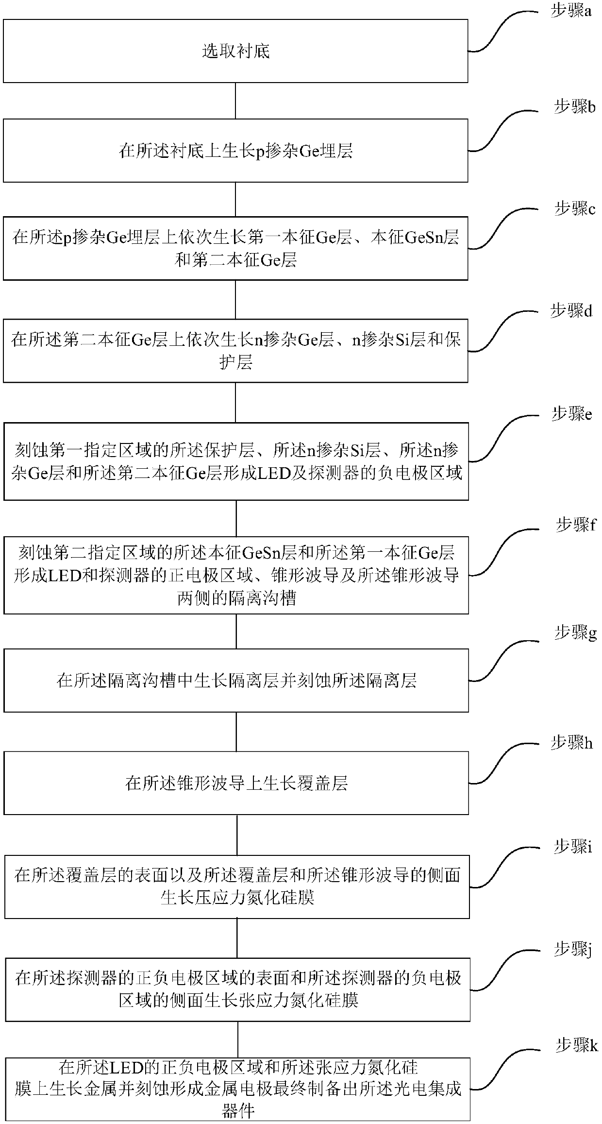
[0065] See figure 1 , figure 1 It is a schematic flowchart of a method for preparing an optoelectronic integrated device provided by an embodiment of the present invention. The method comprises the steps of:

[0066] Step a, select substrate;

[0067] Step b, growing a p-doped Ge buried layer on the substrate;

[0068] Step c, sequentially growing a first intrinsic Ge layer, an intrinsic GeSn layer and a second intrinsic Ge layer on the p-doped Ge buried layer;

[0069] Step d, growing an n-doped Ge layer, an n-doped Si layer and a protective layer sequentially on the second intrinsic Ge layer;

[0070] Step e, etching the protection layer, the n-doped Si layer, the n-doped Ge layer and the second intrinsic Ge layer in the first designated area to form the negative electrode area of ​​the LED and the detector, respectively;

[0071] Step f, etching the intrinsic GeSn layer and the first intrinsic Ge layer in the second specified area to form the p...

Example Embodiment

[0105] Embodiment two

[0106] See Figure 2a ~ Figure 2n , Figure 2a ~ Figure 2n A schematic diagram of the preparation process of an optoelectronic integrated device provided by the embodiment of the present invention. On the basis of the above-mentioned embodiments, this embodiment will introduce the preparation process of the optoelectronic integrated device proposed by the present invention in detail. The method includes:

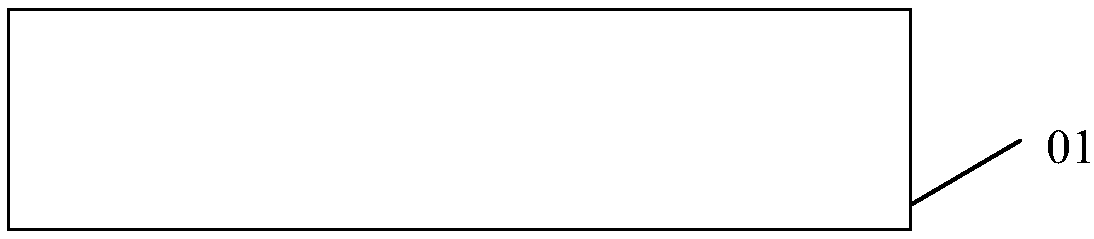
[0107] S101. Substrate selection

[0108] like Figure 2a As shown, the p+ silicon (Si) substrate 01 is selected as the initial material, and the doping concentration is 10 18 cm -3 ;

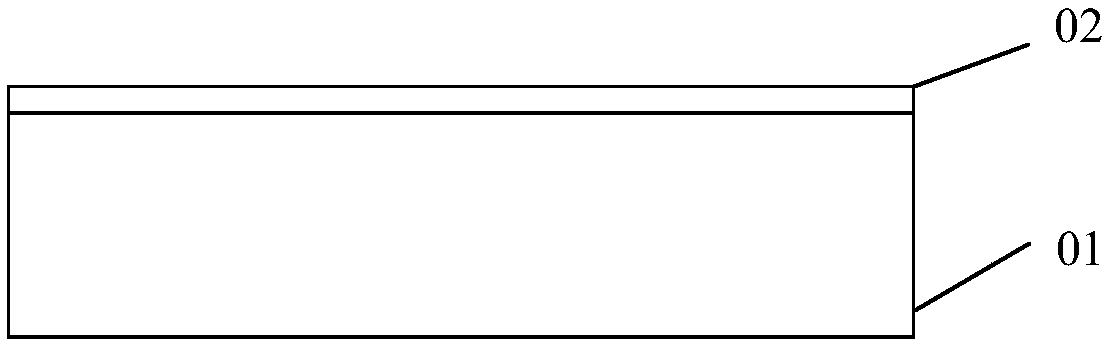
[0109] S102, buried layer growth

[0110] like Figure 2b As shown, at a temperature of 330°C, epitaxial growth with a thickness of 50 nm and a doping concentration of 10 20 cm -3 The p++ doped Ge buried layer 02;

[0111] S103. Growth of the first intrinsic Ge layer

[0112] like Figure 2c As shown, at a temperature of 275° C. to 325° C., a first intrinsic...

Example Embodiment

[0150] Embodiment three

[0151] See image 3 , image 3 It is a schematic diagram of an optoelectronic integrated device provided by an embodiment of the present invention. On the basis of the above embodiments, the present invention also provides an optoelectronic integrated device, wherein the optoelectronic integrated device is formed by the method described in the above embodiment.


PUM

PropertyMeasurementUnit
Thicknessaaaaaaaaaa
Thicknessaaaaaaaaaa
Thicknessaaaaaaaaaa

Abstract

The invention relates to a photoelectric integrated device and a preparation method thereof. The preparation method comprises the following steps of selecting a substrate; sequentially growing a p-doped Ge buried layer, a first intrinsic Ge layer, an intrinsic GeSn layer, a second intrinsic Ge layer, an n-doped Ge layer, an n-doped Si layer and a protective layer on the substrate; etching a firstdesignated area to form the negative electrode areas of an LED and a detector respectively; etching a second designated area to respectively form the positive electrode areas of the LED and the detector, a conical waveguide and the isolation grooves at the two sides of the conical waveguide; growing a covering layer on the conical waveguide; growing a pressure stress silicon nitride film on the whole surface of the covering layer conical waveguide; growing a tensile stress silicon nitride film on the whole surface of the detector; and growing a metal electrode to finally prepare the photoelectric integrated device. According to the present invention, the Si-based modified Ge material is utilized to form the same-layer monolithic photoelectric integrated device of the light-emitting device,the waveguide and the detection device on the Si substrate, the device structure is novel, the device integration degree is high, and the process cost is low.

Description

technical field [0001] The invention relates to the technical field of integrated circuits, in particular to an optoelectronic integrated device and a preparation method thereof. Background technique [0002] With the continuous development of optical communication technology, monolithic optoelectronic integration has become an important solution for high-performance, low-power optoelectronic integrated circuits in the field of computers and communications in the future. In the fields of optical devices, electrical devices and optoelectronic integration, III-V semiconductor materials have been widely used, but their incompatibility with the existing Si process, high production cost and long process cycle restrict their further development. development of. Therefore, finding new materials that are compatible with the current Si process and have good photoelectric properties has become a new hot spot in the semiconductor field. [0003] Ge and Si belong to group IV semicondu...

Claims


Application Information

Patent Timeline
IPC IPC(8): H01L31/18H01L31/0232H01L31/153H01L31/173
CPCH01L31/02327H01L31/153H01L31/173H01L31/1808Y02P70/50
Inventor 薛磊
Owner XIAN CREATION KEJI CO LTD
Why Eureka
Try Eureka