Dark current correction method of CMOS image sensor
A dark current correction and image sensor technology, applied in the field of image processing, can solve the problems of power consumption difference of chip circuit and chip process deviation, and achieve the effect of high correction accuracy and excellent image effect.
- Summary
- Abstract
- Description
- Claims
- Application Information
AI Technical Summary
Problems solved by technology
Method used
Image
Examples
Embodiment Construction
[0031] In order to make the purpose, technical solution and advantages of the present invention clearer, the specific implementation manners of the present invention will be further described in detail below in conjunction with the accompanying drawings.
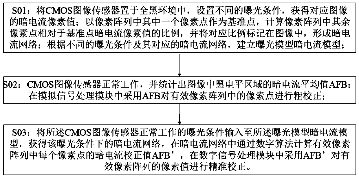
[0032] as attached image 3 As shown, a dark current correction method for a CMOS image sensor provided by the present invention is characterized in that it includes the following steps:
[0033] S01: Place the CMOS image sensor in a completely dark environment, set different exposure conditions, and obtain the dark current pixel value of the corresponding image; use one of the pixels in the pixel array as a reference point, and calculate the relative values of the remaining pixels in the pixel array relative to the reference point Point the ratio of the dark current pixel value, and mark the corresponding ratio in the image to form a dark current network; according to different exposure conditions and their corresponding ...
PUM
 Abstract
Description
Claims
Application Information


