
Three-dimensional organic light-emitting integrated circuit and imaging method

A three-dimensional, integrated circuit technology, applied in the direction of instruments, etc., can solve the problems of self-shading and achieve the effect of long life

Active Publication Date: 2020-07-28
JILIN INST OF RADIO & TELEVISION
View PDF11 Cites 0 Cited by
  • Summary
  • Abstract
  • Description
  • Claims
  • Application Information

AI Technical Summary

Problems solved by technology

[0003] The present invention provides a three-dimensional organic light-emitting integrated circuit and an application system to solve the problems that the existing three-dimensional image is limited inside the display device, and self-shading cannot be realized due to the transparent space.

Method used


Image

  • Three-dimensional organic light-emitting integrated circuit and imaging method
  • Three-dimensional organic light-emitting integrated circuit and imaging method
  • Three-dimensional organic light-emitting integrated circuit and imaging method

Examples


specific Embodiment approach 1

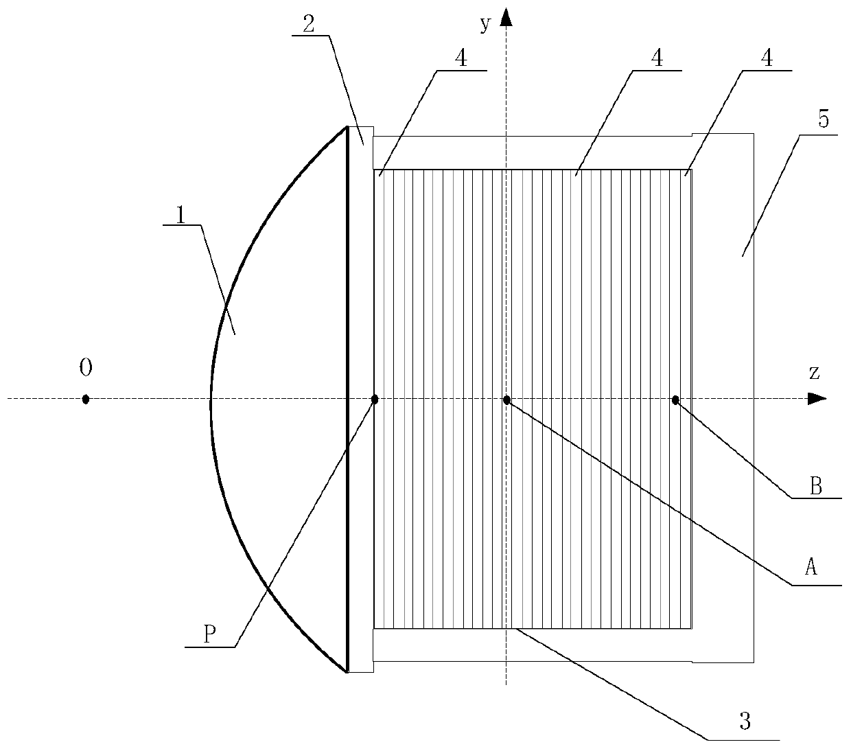
[0020] Specific implementation mode 1. Combination figure 1 and figure 2 To illustrate this embodiment, a three-dimensional organic light emitting integrated circuit includes a convex lens 1, a synchronous diaphragm 2, a three-dimensional light emitter 3 and a light-absorbing housing 5;

[0021] The convex lens 1 is a plano-convex lens, the plane is in contact with the synchronous diaphragm 2, and the line where the main optical axis is located is the z-axis; the z-axis is also the axis of the element, and the direction perpendicular to the z-axis is the y-axis, and the direction perpendicular to the yz plane is the x-axis;

[0022] The focal length of convex lens 1 is S, figure 1 Point A is the right focus of convex lens 1; point B is on the right side of point A, and the distance from point A is also S; point O is the left focus of convex lens 1.

[0023] The synchronous diaphragm 2 adopts a TFT liquid crystal structure and is used as a dot-matrix optical switch, and has...

specific Embodiment approach 2

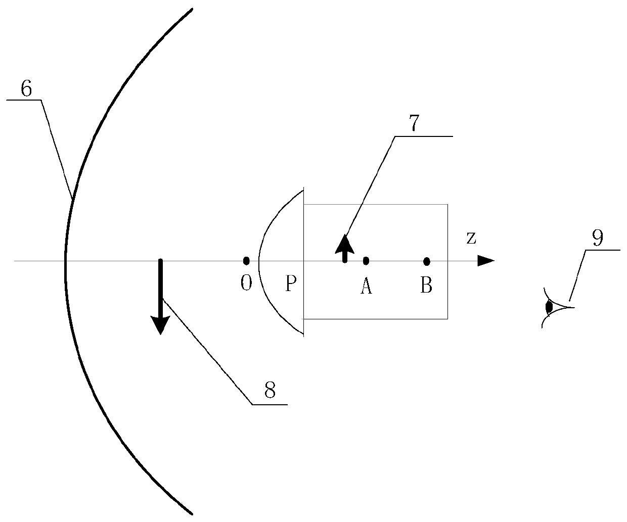
[0033] Specific embodiment two, combine Figure 3 to Figure 5 To illustrate this embodiment, the imaging method of a three-dimensional organic light-emitting integrated circuit is applied, and the specific process of the method is as follows:

[0034] First, the concave reflector 6 and the three-dimensional organic light emitting integrated circuit are coaxially arranged to form an imaging system, the focal length of the concave reflector 6 is F, and the right intersection point coincides with the left focus of the three-dimensional organic light emitting integrated circuit at point O;

[0035] The original image 7 in the three-dimensional light-emitting body in the three-dimensional organic light-emitting integrated circuit, the light is emitted by the concave mirror 6 to form an image 8; the human eye 9 can see this image 8 from the opposite direction of the z-axis;

[0036] If the z-axis coordinate of the original image 7 to point A is Z, then the coordinate R of image 8 on...


PUM


Abstract

The invention discloses a three-dimensional organic light-emitting integrated circuit and an imaging method and relates to the field of broadcast televisions, computer image processing and integratedcircuits, and aims to solve the problem that an existing three-dimensional image is limited in a display device and cannot be shielded due to transparent space. The three-dimensional organic light-emitting integrated circuit comprises a convex lens, a synchronous diaphragm, a three-dimensional light-emitting body and a light absorption shell which are sequentially arranged along a main optical axis; the convex lens is a plano-convex lens; the plane of the plano-convex lens is connected with the synchronous diaphragm; the three-dimensional light-emitting body is arranged in the light absorptionshell and connected with the synchronous diaphragm; the two sides of the opening end of the light absorption shell are connected with the synchronous diaphragm through light-transmitting glue; the plano-convex lens is larger than the inner edge of the opening end of the light absorption shell; and all gaps among the convex lens, the synchronous diaphragm, the three-dimensional light-emitting bodyand the light absorption shell are filled with light-transmitting glue. According to the imaging method, a naked eye three-dimensional display device can be manufactured, and a three-dimensional object with a real visual angle can be dynamically displayed in the air.

Description

technical field [0001] The invention relates to the fields of radio and television, computer image processing and integrated circuits, in particular to a three-dimensional organic light-emitting integrated circuit and an application system. Background technique [0002] Naked-eye 3D display of video images is a research hotspot. At present, mainstream 3D display technologies are generally divided into parallax type, light field reconstruction type, holographic type, and volumetric 3D type; The same, it belongs to pseudo three-dimensional display, and other types can realize true three-dimensional display; light field reconstruction type needs precise mechanical movement mechanism to cooperate with multiple optical devices, and the structure is more complicated; holographic type can realize some static image display at present, but limited by space Due to the limitation of light modulation components and computing power, dynamic holography still has difficulties in the short ...

Claims


Application Information

Patent Timeline
Patent Type & Authority Applications(China)
IPC IPC(8): G02B30/56
Inventor 焦杰
Owner JILIN INST OF RADIO & TELEVISION
Learn More