
Power device and preparation method thereof

A technology for power devices and light modulation, which can be used in electrical components, cold cathode manufacturing, electrode system manufacturing, etc., and can solve problems such as low reliability

Pending Publication Date: 2020-07-31
INST OF MICROELECTRONICS CHINESE ACAD OF SCI
View PDF0 Cites 1 Cited by
  • Summary
  • Abstract
  • Description
  • Claims
  • Application Information

AI Technical Summary

Problems solved by technology

[0003] The embodiment of the present application solves the technical problem of low reliability of existing power devices by providing a power device and its preparation method

Method used


Image

  • Power device and preparation method thereof
  • Power device and preparation method thereof
  • Power device and preparation method thereof

Examples


Embodiment 1

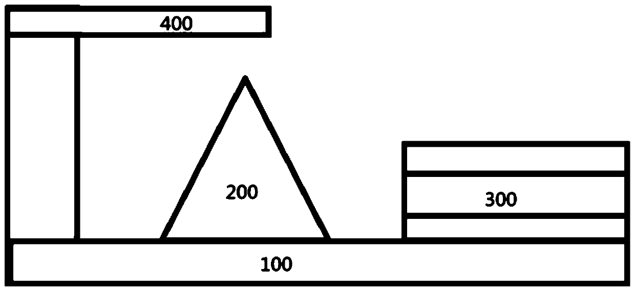
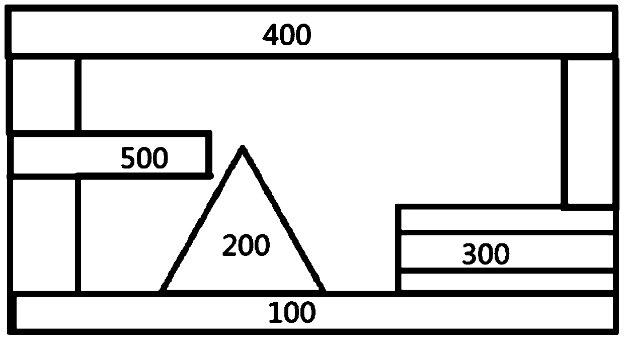
[0044] Such as figure 1 As shown, the present application provides a power device through an embodiment, including at least one vacuum-packaged unit structure; wherein, the unit structure includes:

[0045] Silicon substrate 100;

[0046] Forming the emitter 200 on the silicon substrate 100 using a silicon-based process;

[0047] A light modulator 300 formed on the silicon substrate 100 by a silicon-based process, the light modulator 300 is used to generate photons to excite the emitter 200 to emit electrons;

[0048] The collector 400 is formed on the silicon substrate 100 by using a silicon-based process, and the collector 400 is used to excite and receive electrons emitted by the emitter 200 .

[0049] It should be noted that the power device of this embodiment generally includes a plurality of integrated unit structures, and the internal structure of a single unit structure is firstly described here.

[0050] see figure 1, the silicon substrate 100 is located at the bo...

Embodiment 2

[0073] Based on the same inventive concept as in Embodiment 1, see Figure 5 , this embodiment provides a method for preparing a power device, the method is used to prepare the unit structure in Embodiment 1; the method includes:

[0074] S102, preparing and obtaining a silicon substrate;

[0075] S104. Epitaxially prepare an optical modulation electrode on a silicon substrate, the negative electrode of the optical modulation electrode is connected to the silicon substrate, and the positive electrode of the optical modulation electrode is drawn out as an optical modulation control electrode;

[0076] S106. Prepare an emitter on the silicon substrate next to the light modulation electrode;

[0077] S108 , combining the prepared collector with the silicon substrate through a silicon wafer bonding process to form a unit structure.

[0078] It should be noted that, for the specific implementation manner of this embodiment, please refer to Embodiment 1, which will not be repeated...


PUM


Abstract

The invention discloses a power device, which comprises at least one vacuum-packaged unit structure, wherein the unit structure comprises a silicon substrate, and an emitting electrode, a light modulation electrode and a collecting electrode which are formed on the silicon substrate. According to the invention, the whole device is prepared by adopting a unified silicon-based process, so that the problem of inconsistency of emitters of traditional cold cathode field emission in a preparation process is solved, the internal precision and consistency of the device are improved, and the reliability of the device is enhanced; and a light modulation electrode formed on a silicon substrate is introduced based on a silicon-based process, so that the field emission efficiency of the emitter is enhanced, the inconsistency of the distance between the tip of the emitter and the collector caused by the non-uniformity of the emitter is counteracted, the process redundancy of the cold cathode emitting electrode is increased, the device does not need to completely depend on the field emission principle to generate electrons, the field emission load is reduced, and the reliability of the device isfurther enhanced.

Description

technical field [0001] The invention relates to the technical field of vacuum microelectronics, in particular to a power device and a preparation method thereof. Background technique [0002] The withstand voltage of existing power devices is borne by the space electric field of semiconductor junctions (eg, PN junctions), which limits the on-resistance and working efficiency of the devices. Although the existing field cathode emission vacuum microelectronic power devices can improve the withstand voltage capability of the power device, because its electron emission is completely dependent on electric field emission, its power and reliability cannot be guaranteed, so the product is not Mature. Contents of the invention [0003] Embodiments of the present application solve the technical problem of low reliability of existing power devices by providing a power device and a manufacturing method thereof. [0004] On the one hand, the present application provides the following...

Claims


Application Information

Patent Timeline
IPC IPC(8): H01J19/24H01J19/28H01J19/42H01J9/02H01J9/14
CPCH01J19/24H01J19/28H01J19/42H01J9/025H01J9/14H01J2209/0223
Inventor 赵发展卜建辉罗家俊
Owner INST OF MICROELECTRONICS CHINESE ACAD OF SCI
Learn More