Semi-floating gate memory based on two-dimensional material and preparation method thereof

A two-dimensional material and semi-floating gate technology, which is applied in semiconductor devices, electrical solid devices, electrical components, etc., can solve the problems of slow writing operation, limited application, and data retention ability of only milliseconds, so as to increase data retention time , Reduce interface defects and improve device reliability

Active Publication Date: 2020-08-04
FUDAN UNIV +1
View PDF7 Cites 5 Cited by
  • Summary
  • Abstract
  • Description
  • Claims
  • Application Information

AI Technical Summary

Problems solved by technology

Volatile memory has a write speed of nanoseconds, but its data retention capability is only milliseconds, so it can only be used in limited storage areas such as caches
For non-volatile storage technologies, such as flash memory technology, its data retention capacity can reach 10 years, but the relatively slow write operation greatly limits its application in the cache field

Method used


Image

  • Semi-floating gate memory based on two-dimensional material and preparation method thereof
  • Semi-floating gate memory based on two-dimensional material and preparation method thereof
  • Semi-floating gate memory based on two-dimensional material and preparation method thereof

Examples


Embodiment Construction

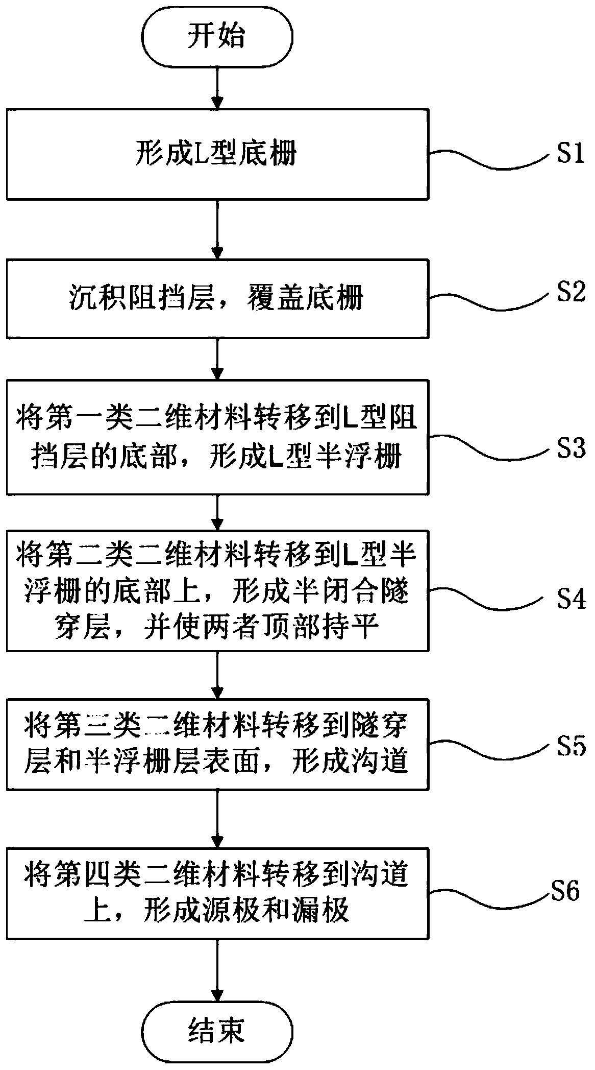
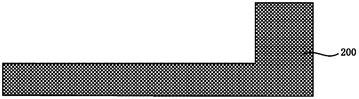
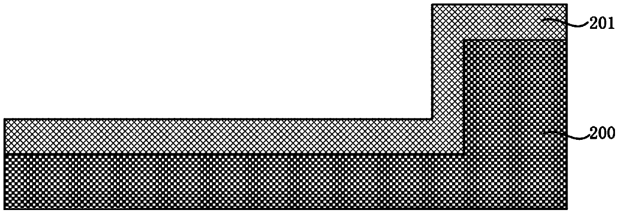
[0036] The present invention will be further introduced below in conjunction with the embodiments and accompanying drawings. It should be understood that the examples are only used to explain the present invention, not to limit the present invention. All other embodiments obtained by persons of ordinary skill in the art without creative efforts fall within the protection scope of the present invention.

[0037] In the description of the present invention, it should be noted that the orientation or positional relationship indicated by the terms "upper", "lower", "vertical" and "horizontal" are based on the orientation or positional relationship shown in the drawings, and are only for convenience The present invention is described and simplified descriptions do not indicate or imply that the device or element referred to must have a specific orientation, be constructed and operate in a specific orientation, and thus should not be construed as limiting the present invention. In ...


PUM


Abstract

The invention belongs to the technical field of semiconductor memories, and particularly relates to a semi-floating gate memory based on a two-dimensional material and a preparation method thereof. The semi-floating gate memory comprises an L-shaped bottom gate, a barrier layer covering the surface of the bottom gate, and an L-shaped semi-floating gate layer which is a first type of two-dimensional material, and the top of the L-shaped semi-floating gate layer is flush with the top of the bottom gate; the semi-floating gate memory further comprises a semi-closed tunneling layer at the bottom of the semi-floating gate, wherein the semi-closed tunneling layer is a second type of two-dimensional material, and the upper surface of the semi-closed tunneling layer is flush with the top of the semi-floating gate; the semi-floating gate memory further comprises a channel layer which covers the semi-floating gate and the semi-closed tunneling layer and is made of a third type two-dimensional material, and the upper surface of the channel layer is flush with the top of the barrier layer; the semi-floating gate memory further comprises a source electrode and a drain electrode which are on thesurface of the channel and are a fourth type of two-dimensional material. The first type of two-dimensional material and the third type of two-dimensional material form a diode, and the first type oftwo-dimensional material, the third type of two-dimensional material, the barrier layer and the bottom gate form a grid-control diode. The device is good in reliability and high in data erasing and writing speed, and the data retention time can be prolonged; in addition, the device is small in size and suitable for being used in ultrathin electronic equipment.

Description

technical field [0001] The invention belongs to the technical field of semiconductor memory, and in particular relates to a semi-floating gate memory based on two-dimensional materials and a preparation method thereof. Background technique [0002] Today's mainstream storage technology is divided into two categories: volatile storage technology and non-volatile storage technology. For volatile storage technologies, mainly static random access memory SRAM and dynamic random access memory DRAM. Volatile memory has a write speed of nanoseconds, but its data retention capability is only milliseconds, so it can only be used in limited storage areas such as caches. For non-volatile storage technologies, such as flash memory technology, its data retention capability can reach 10 years, but relatively slow write operations greatly limit its application in the cache field. On the other hand, two-dimensional materials, such as transition metal sulfides, not only have high mobility, ...

Claims


Application Information

Patent Timeline
Patent Type & Authority Applications(China)
IPC IPC(8): H01L27/105H01L29/24H01L29/417H01L29/43
CPCH01L29/24H01L29/41725H01L29/43H10B99/00
Inventor 朱宝陈琳孙清清张卫
Owner FUDAN UNIV
Why Eureka
Try Eureka