Composite electrode structure and light emitting device

A light-emitting device and composite electrode technology, which is applied in the direction of electric solid-state devices, electrical components, semiconductor devices, etc., can solve the problems of affecting the luminous efficiency of light-emitting devices and aggravating the decline of devices, so as to solve the problems of accelerating device decline, promoting electron-hole balance, The effect of avoiding recession

Active Publication Date: 2021-07-20
GUANGDONG JUHUA PRINTING DISPLAY TECH CO LTD
View PDF9 Cites 0 Cited by
  • Summary
  • Abstract
  • Description
  • Claims
  • Application Information

AI Technical Summary

Problems solved by technology

However, in the long-term use of these light-emitting devices, there will still be aggravated degradation of the device, which will seriously affect the luminous efficiency and service life of the light-emitting device.

Method used


Image

  • Composite electrode structure and light emitting device
  • Composite electrode structure and light emitting device
  • Composite electrode structure and light emitting device

Examples


Embodiment 1

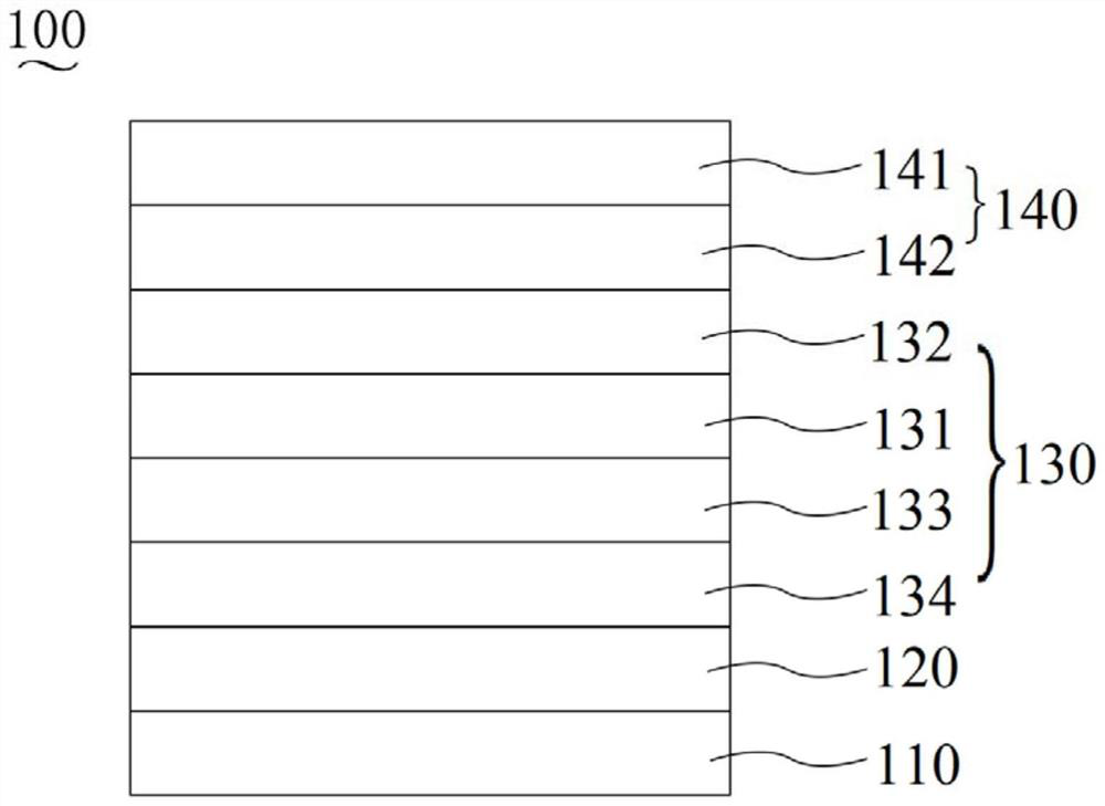
[0068] (1) Using transparent conductive film ITO as the anode, the thickness is 50nm;

[0069] (2) Depositing PEDOT by solution method on the anode:PSS is used as a hole injection layer with a thickness of 30nm;

[0070] (3) Utilizing solution method to deposit TFI on the hole injection layer as the hole transport layer, the thickness is 30nm;

[0071] (4) Depositing CdSe / ZnS as a quantum dot luminescent layer by a solution method on the hole transport layer, with a thickness of 25nm;

[0072] (5) Utilizing solution method to deposit ZnO on the quantum dot luminescent layer as the electron transport layer, the thickness is 40nm;

[0073] (6) Evaporating Cu on the electron transport layer is an electrode protection layer with a thickness of 5nm;

[0074] (7) Evaporating Al on the electrode protection layer as the Al metal electrode layer, with a thickness of 100nm;

[0075] (8) Place the above-mentioned QLED on a baking tray, and bake at 120° C. for 30 minutes.

Embodiment 2

[0077] (1) Using transparent conductive film ITO as the anode, the thickness is 50nm;

[0078] (2) Depositing PEDOT by solution method on the anode:PSS is used as a hole injection layer with a thickness of 30nm;

[0079] (3) Utilizing solution method to deposit TFI on the hole injection layer as the hole transport layer, the thickness is 30nm;

[0080] (4) Depositing CdSe / ZnS as a quantum dot luminescent layer by a solution method on the hole transport layer, with a thickness of 25nm;

[0081] (5) Utilizing solution method to deposit ZnO on the quantum dot luminescent layer as the electron transport layer, the thickness is 40nm;

[0082] (6) Evaporating Zn on the electron transport layer as an electrode protection layer, with a thickness of 5nm;

[0083] (7) Evaporating Al on the electrode protection layer as the Al metal electrode layer, with a thickness of 100nm;

[0084] (8) Place the above-mentioned QLED on a baking tray, and bake at 120° C. for 30 minutes.

Embodiment 3

[0086] (1) Using transparent conductive film ITO as the anode, the thickness is 50nm;

[0087] (2) Depositing PEDOT by solution method on the anode:PSS is used as a hole injection layer with a thickness of 30nm;

[0088] (3) Utilizing solution method to deposit TFI on the hole injection layer as the hole transport layer, the thickness is 30nm;

[0089] (4) Depositing CdSe / ZnS as a quantum dot luminescent layer by a solution method on the hole transport layer, with a thickness of 25nm;

[0090] (5) Utilizing solution method to deposit ZnO on the quantum dot luminescent layer as the electron transport layer, the thickness is 40nm;

[0091] (6) Evaporating Ag on the electron transport layer as an electrode protection layer, with a thickness of 5nm;

[0092] (7) Evaporating Al on the electrode protection layer as the Al metal electrode layer, with a thickness of 100nm;

[0093] (8) Place the above-mentioned QLED on a baking tray, and bake at 120° C. for 30 minutes.


PUM

PropertyMeasurementUnit
electron work functionaaaaaaaaaa
thicknessaaaaaaaaaa
thicknessaaaaaaaaaa

Abstract

The present invention relates to a composite electrode structure and a light-emitting device. The composite electrode structure includes an electrode main body layer and an electrode protection layer for protecting the electrode main body layer. The electrode protection layer and the electrode main body layer are laminated. The main body layer of the electrode contains metal elements of group IIIA, and the electrode protection layer is a metal layer formed of metal elements of group IAIIIA or a metal layer of metal elements of group IIIIII or of metal elements of group IAIIIA and group IIIIII. Various alloy layers formed. The composite electrode structure is applied to the electrodes of light-emitting devices. Since the electrode protection layer itself has a barrier function, it can protect the main body layer of the electrode. Therefore, the luminous efficiency and service life of the light-emitting device can be improved to a certain extent.

Description

technical field [0001] The invention relates to the technical field of light-emitting display, in particular to a compound electrode structure and a light-emitting device. Background technique [0002] Due to the unique optical properties of quantum dots, such as continuously adjustable emission wavelength with size and composition, narrow emission spectrum, high fluorescence efficiency, and good stability, quantum dot-based electroluminescent diodes (QLEDs) have been widely used in the display field. Follow and research. In addition, QLED also has many advantages that cannot be realized by LCD (liquid crystal display), such as large viewing angle, high contrast ratio, fast response speed, and flexibility, so it is expected to become the next generation of display technology. [0003] After decades of development, the performance of QLEDs has made great progress, one of the important reasons is the use of ZnO nanoparticles as electron transport materials. This is because: ...

Claims


Application Information

Patent Timeline
Patent Type & Authority Patents(China)
IPC IPC(8): H01L33/40H01L51/52
CPCH01L33/40H10K50/82
Inventor 苏亮
Owner GUANGDONG JUHUA PRINTING DISPLAY TECH CO LTD
Why Eureka
Try Eureka