Thus, when thermal noises are generated in the p-type epitaxial layer, they are input to the base-bonding pad through a parasitic capacitance produced due to the insulation layer which serves as a dielectric, resulting in decline in a noise factor (NF) characteristic of the BJT.
Method used
Image
Click on the blue label to locate the original text in one second.
Reading with bidirectional positioning of images and text.
Examples
first embodiment
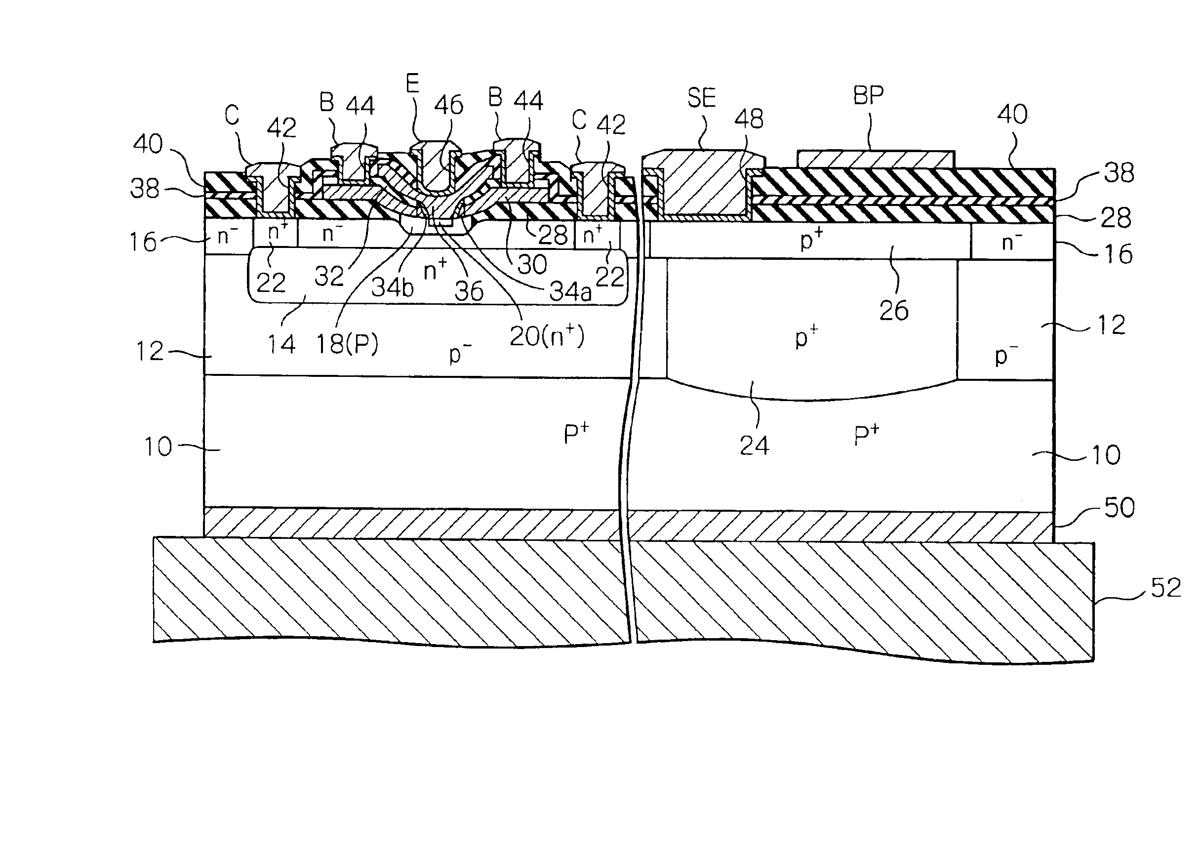
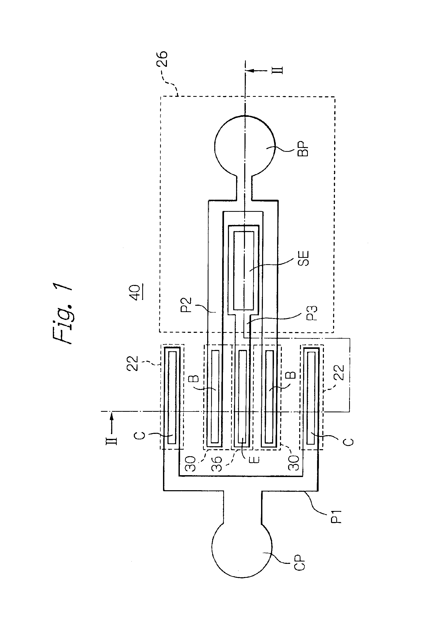
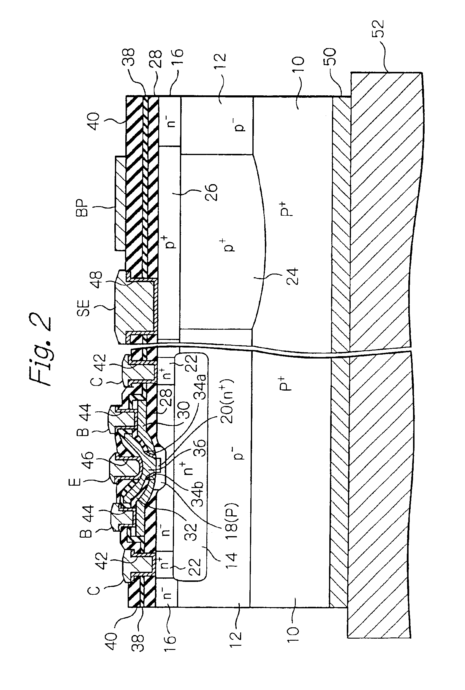
[0056]Referring to FIGS. 1, 2, and 3, a semiconductor device including a bipolar junction transistor (BJT) according to the present invention is shown. Note, FIG. 1 shows the semiconductor device as a plan view, and FIG. 2 shows a cross section of the semiconductor device, taken along the II—II line of FIG. 1.
[0057]As shown in FIG. 2, the semiconductor device includes a high concentration / low resistance p+-type substrate 10, which is derived from a p+-type diffusion layer formed on a siliconwafer (not shown), and a low concentration / high resistance p−-type epitaxial layer 12 formed on the high concentration / low resistance p+-type substrate 10. A high concentration / low resistance n+-type collector-buried region 14 is formed in an element-formation area previously defined on the p−-type epitaxial layer 12.
[0058]The semiconductor device also includes a low concentration / high resistance n−-type epitaxial layer 16 formed on the p−-type epitaxial layer 12 having the n+-type collector-bur...
second embodiment
[0093]FIG. 25 shows the semiconductor device including the bipolar junction transistor (BJT) according to the present invention. Note, in this drawing, the features similar to those of FIG. 2 are indicated by the same references.
[0094]In the second embodiment, when a part of the first polycrystalline silicon layer 30 is left on the first insulation layer 28 as shown in FIG. 23, another part 30a of the first polycrystalline silicon layer 30 is left on the first insulation layer 28 as a conductive layer so as to cover the p+-type sub-emitter region 26, as shown in FIG. 25, and thus the base-bonding pad BP is encompassed with the left part or conductive layer 30a of the first polycrystalline silicon layer 30.
[0095]As is apparent from FIG. 25, the conductive layer 30a is electrically connected to the barrier metal layer 48, and therefore, the sub-emitter electrode SE. Namely, the conductive layer 30a is grounded through the intermediary of the sub-emitter electrode SE, the p+-type sub-e...
third embodiment
[0100]FIG. 28 shows the semiconductor device including the bipolar junction transistor (BJT) according to the present invention. Note, in this drawing, the features similar to those of FIG. 2 are indicated by the same references.
[0101]In this third embodiment, a p+-type channel stopper region 26a is formed in the n−-type epitaxial layer 16 to cover the p+-type diffusion buried layer 24, and a field silicon dioxide layer 78 is then formed on the p+-type channel, using a Local Oxidation of Silicon (LOCOS) method. Then, a first insulation layer 28 and a first polycrystalline silicon layer 30 are formed and laminated in order on the n−-type epitaxial layer 16 having the field silicon dioxide layer 78, and are processed in substantially the same manner as in the above-mentioned first embodiment. Subsequently, a second insulation layer 32 and a second polycrystalline silicon layer 36 are formed and laminated in order on the first polycrystalline silicon layer, and are processed in substan...
PUM
Abstract
A semiconductor device includes a low resistancesemiconductor substrate, a high resistancesemiconductor layer formed on the substrate, an insulation layer formed on the semiconductor layer, and a transistor element composed of a collector region, abase region, and an emitter region formed in the semiconductor layer. The device further includes an emitter electrode formed in the insulation layer to be connected to the emitter region, a sub-emitter electrode formed in the insulation layer connected to the emitter electrode, a low resistanceimpurity-diffusion region formed in the semiconductor layer such that the sub-emitter electrode is connected to the substrate through the impurity-diffusion region, a base electrode formed in the insulation layer to be connected to the base region, and a base-bonding pad formed on the insulation layer to be connected to the base electrode. The base-bonding pad is placed on the insulation layer above the impurity-diffusion region to be at least partially encompassed with the impurity-diffusion region.
Description
BACKGROUND OF THE INVENTION[0001]1. Field of the Invention[0002]The present invention relates to a semiconductor device including a bipolar junction transistor, and a production method for producing such a semiconductor device.[0003]2. Description of the Related Art[0004]As a representative type of bipolar junction transistor (BJT), an emitter-grounded type high frequency BJT is well known. For example, the emitter-grounded type high frequency BJT is disclosed in Japanese Laid-Open Patent Publications (KOKAI) No. SHO-64-073669 and No. HEI-10-247713.[0005]As disclosed in these publications by way of example, the emitter-grounded type high frequency BJT comprises a p+-type substrate, a p−-type epitaxial layer formed on the p+-type substrate, and an n−-type epitaxial layer formed on the p+-type substrate. The p−-type epitaxial layer has a collector-buried region formed therein, and the n−-type epitaxial layer has a collector-contact region formed therein and electrically connected to t...
Claims
Application Information
Patent Timeline
Application Date:The date an application was filed.
Publication Date:The date a patent or application was officially published.
First Publication Date:The earliest publication date of a patent with the same application number.
Issue Date:Publication date of the patent grant document.
PCT Entry Date:The Entry date of PCT National Phase.
Estimated Expiry Date:The statutory expiry date of a patent right according to the Patent Law, and it is the longest term of protection that the patent right can achieve without the termination of the patent right due to other reasons(Term extension factor has been taken into account ).
Invalid Date:Actual expiry date is based on effective date or publication date of legal transaction data of invalid patent.

