PCB and automatic machining equipment and method thereof

A kind of PCB circuit board, automatic processing technology, applied in lighting and heating equipment, printed circuit, printed circuit manufacturing and other directions, can solve the problems of poor PCB circuit board processing efficiency, increase turnover efficiency and turnover matching degree.

Active Publication Date: 2020-08-07
深圳捷多邦科技有限公司
View PDF6 Cites 9 Cited by
  • Summary
  • Abstract
  • Description
  • Claims
  • Application Information

AI Technical Summary

Problems solved by technology

[0005] The object of the present invention is to solve the above-mentioned problem of poor processing efficiency of the existing PCB circuit boards, and provide a method to facilitate the simultaneous transportation of multiple PCB circuit boards through the feeding device and improve the transportation efficiency; it is convenient to detect the front and back sides through the positioning detection device , It is convenient to save the space occupied by the device, and the structure is simple to increase the turning efficiency and the turning fit; the laser marking device is convenient to directly carry out double-sided marking processing of the PCB circuit board, without transporting to the marking processing place for unified processing, and improving the marking efficiency; Through the conveying connection device, it is convenient to convert multiple simultaneously conveyed PCB circuit boards into single conveying, which is convenient for subsequent labeling processing, and improves the fluency of the overall processing and the overall processing efficiency of a PCB circuit board automatic processing equipment.

Method used


Image

  • PCB and automatic machining equipment and method thereof
  • PCB and automatic machining equipment and method thereof
  • PCB and automatic machining equipment and method thereof

Examples


Embodiment Construction

[0034] The specific implementation manner of the present invention will be described in detail below in conjunction with the accompanying drawings.

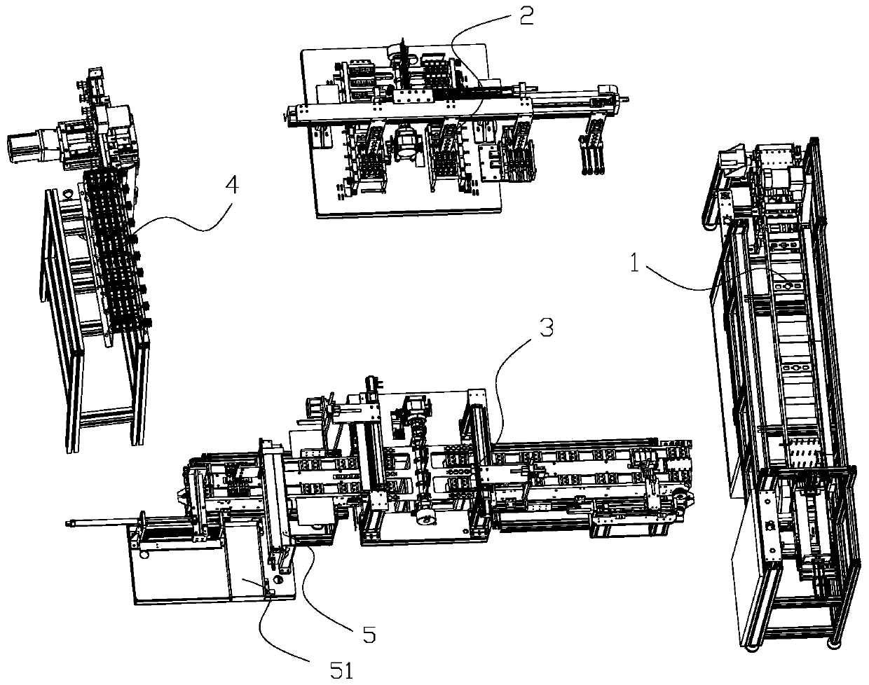
[0035] like figure 1 As shown, a PCB circuit board automatic processing equipment, the equipment includes a feeding device 1, a positioning detection device 2, a laser marking device 3 and a conveying connection device 4; The positioning detection device 2, the laser marking device 3 and the conveying connection device 4 are sequentially connected to each other; the feeding device 1 is used to transport multiple circuit boards to the positioning detection device 2, and the positioning detection device 2 is used to carry out multiple circuit boards. Positioning and front and back detection, and transfer multiple circuit boards to the laser marking device 3. The laser marking device 3 is used to perform laser laser processing on the circuit boards and transport them to the transport joint device 4. The transport joint device 4 is u...


PUM


Abstract

The invention relates to the technical field of PCB machining. Automatic machining equipment of PCBs comprises a feeding device, a positioning detection device, a laser marking device and a conveyingjoining device, wherein the feeding device is used for conveying a plurality of circuit boards to the positioning detection device, the positioning detection device is used for positioning the plurality of circuit boards, detecting front and back surfaces of the plurality of circuit boards and transferring the plurality of circuit boards to the laser marking device, the laser marking device is used for carrying out laser processing on the circuit boards and conveying the circuit boards to the conveying joining device, and the conveying joining device is used for converting multi-block conveying of the circuit boards into single-block conveying for subsequent labeling processing. The device has the advantages that multiple blocks of circuit boards are conveyed at the same time, the conveying efficiency is improved, front face and back face detection and overturning are facilitated, and the overturning efficiency and the laser efficiency are improved; and the continuity of the whole processing production line is improved.

Description

technical field [0001] The invention relates to the technical field of PCB circuit board processing, in particular to an automatic PCB circuit board processing device and a method thereof. Background technique [0002] PCB, the Chinese name is printed circuit board, also known as printed circuit board, is an important electronic component, a support for electronic components, and a carrier for electrical connections of electronic components. The precision requirements in the process of marking the surface of the PCB circuit board are very high. It is required to mark clear text, model, manufacturer and other information without damaging the components, and the PCB circuit board is marked. Finally, it is necessary to paste the qualified label before cutting the material. [0003] Existing automatic processing equipment for PCB circuit boards, such as the processing equipment disclosed in the Chinese utility model patent whose publication number is CN207736986U, is a kind of ...

Claims


Application Information

Patent Timeline
Patent Type & Authority Applications(China)
IPC IPC(8): B65G49/06B65G37/00H05K3/00H05K1/00B65C9/02
CPCB65C9/02B65G37/00B65G49/06B65G49/061B65G49/067H05K1/00H05K3/00
Inventor 徐建方万爱花王富生
Owner 深圳捷多邦科技有限公司
Why Eureka
Try Eureka