GGNMOS ESD protection device structure based on SOI process

A technology for protecting devices and processes, which is applied in the field of GGNMOSESD protection device structures, can solve problems such as rising ratios, achieve full body contact, save area, and improve ESD resistance

Active Publication Date: 2020-08-07
58TH RES INST OF CETC
View PDF4 Cites 4 Cited by
  • Summary
  • Abstract
  • Description
  • Claims
  • Application Information

AI Technical Summary

Problems solved by technology

[0004] The object of the present invention is to provide a kind of GGNMOS ESD protection device structure based on SOI process, to solve the failure caused by ESD in the above-mentioned background technology and account for more than 37% in the failure of integrated circuits, and this ratio increases with the device The shrinking feature size is further raising the issue

Method used


Image

  • GGNMOS ESD protection device structure based on SOI process
  • GGNMOS ESD protection device structure based on SOI process
  • GGNMOS ESD protection device structure based on SOI process

Examples


Embodiment Construction

[0018] In order to solve the problem that the failure caused by ESD accounts for more than 37% of the failures of integrated circuits, and this proportion is further increasing with the reduction of device feature size, a GGNMOS ESD protection device structure based on SOI process is proposed. The following will clearly and completely describe the technical solutions in the embodiments of the present invention with reference to the accompanying drawings in the embodiments of the present invention. Obviously, the described embodiments are only some, not all, embodiments of the present invention. Based on the embodiments of the present invention, all other embodiments obtained by persons of ordinary skill in the art without making creative efforts belong to the protection scope of the present invention.

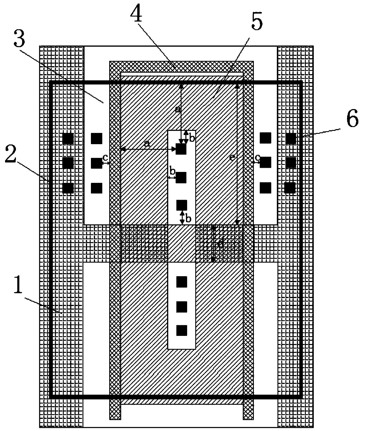
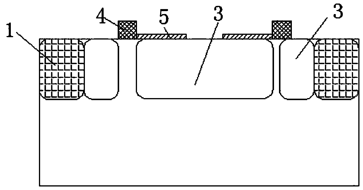
[0019] see figure 1 , this embodiment provides a GGNMOS ESD protection device structure based on SOI process, including SAB layer 5, P-type doped source and drain SP1, N-type d...


PUM


Abstract

The invention discloses a GGNMOS ESD protection device structure based on an SOI technology. The structure comprises an SAB layer, P-type doped source-drain units SP, N-type doped source-drain units SN, a polycrystalline gate POLY, a device active region TO and contact holes W1. P-type doped source and drain units of a strip-type NMOS tube are segmented; the body contact of the device is designedbetween every two sections of P-type doped source-drain units. A P-type doped source and a P-type doped drain of a strip-type NMOS tube are segmented; the body contact of the device is designed between every two P-type doped source drains, the N-type doped source drain units of the strip-type NMOS tube are ingeniously segmented through the structure, the range of an SN injection layer and the range of an SP injection layer are defined by the segments respectively, the process is achieved through photoetching, and by means of the design, on one hand, the area is saved, and on the other hand, the body contact is more sufficient; TLP test evaluation shows that under the same area, the ESD resistance of the SOI GGNMOS device is obviously improved by 1.2 times or above compared with that of a traditional SOI GGNMOS device.

Description

technical field [0001] The invention relates to the technical field of semiconductor integrated circuits, in particular to a GGNMOS ESD protection device structure based on SOI technology. Background technique [0002] ESD protection technology has been the focus of research in the field of microelectronics. According to statistics, failures caused by ESD account for more than 37% of integrated circuit failures, and this proportion is further increasing with the reduction of device feature size. [0003] The characteristics of high speed, low leakage, good sub-threshold characteristics, latch-up immunity and low soft error rate provided by SOI technology have made it one of the most competitive technologies widely used. Since the bottom of the SOI device is isolated by a thick buried oxide layer, and the surroundings of the device are also fully dielectrically isolated by SiO2, SOI devices and circuits are very sensitive to ESD stress on the one hand; on the other hand, com...

Claims


Application Information

Patent Timeline
Patent Type & Authority Applications(China)
IPC IPC(8): H01L27/02
CPCH01L27/0296H01L27/0292H01L27/0266
Inventor 顾祥张庆东纪旭明郑重
Owner 58TH RES INST OF CETC
Why Eureka
Try Eureka