A kind of LED full-color display panel and packaging method thereof

A technology of full-color display and packaging method, applied in the manufacturing of semiconductor devices, electrical components, semiconductor/solid-state devices, etc., can solve the problems of difficult calibration, low product yield, and high price, so as to reduce manufacturing difficulty and cost, and simplify inspection. Process, the effect of reducing complexity

Active Publication Date: 2021-09-17
ZHEJIANG INTELED OPTOELECTRONICS TECH
View PDF5 Cites 0 Cited by
  • Summary
  • Abstract
  • Description
  • Claims
  • Application Information

AI Technical Summary

Problems solved by technology

[0005] The present invention mainly solves the problems of complex PCB substrate design, low product yield and high price in the prior art; and the traditional COB cannot mix light and difficult to calibrate; it provides a LED full-color display panel and its packaging method, using CSP devices as the minimum unit, the hierarchical design of CSP devices is simple, the product yield rate can be improved, and light and color can be mixed

Method used


Image

  • A kind of LED full-color display panel and packaging method thereof
  • A kind of LED full-color display panel and packaging method thereof

Examples


Embodiment

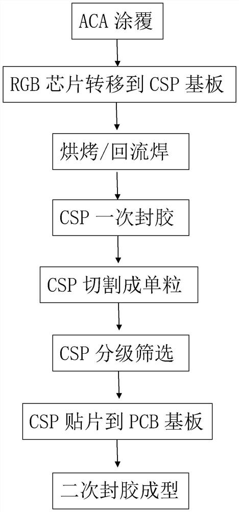
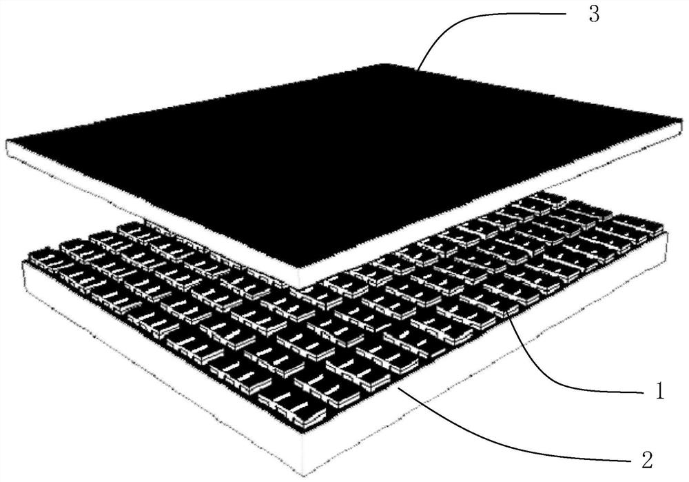
[0034] A kind of LED full-color display panel packaging method, such as figure 1 shown, including the following steps:

[0035] S1: Use ACA welding technology to seal the CSP device once, and cut the CSP device into single grains.

[0036] S11: Coating ACA on the CSP substrate.

[0037] ACA (Anisotropic Conductive Adhesive) is able to conduct electricity in the longitudinal direction, but not in the transverse direction. Therefore, the spacing between the light-emitting units can be greatly seen, and the use of ACA soldering technology instead of traditional solder paste printing can solve the problem that the yield rate of solder paste printed with small spacing is difficult to guarantee, and the cost is lower than that of using solder paste printing. During ACA coating, only one layer of ACA needs to be coated on the substrate, the coating process is convenient, the equipment used has no precision requirements, and the cost of the equipment is low.

[0038] Using ACA sold...


PUM


Abstract

The invention discloses an LED full-color display panel and a packaging method thereof. In order to overcome the problems of complicated PCB substrate design, low product yield and high price in the prior art; and the traditional COB cannot mix light and make calibration difficult; the present invention adopts the following steps: S1: use ACA welding technology to seal the CSP device once, Cut the CSP device into single grains; S2: use the spectroscopic equipment to classify and screen the cut CSP devices, and screen and remove the CSP devices with poor electrical properties; S3: mount the screened single grain CSP devices on the PCB substrate, and mix Mix lamps with lamps, and use the chromaticity correction system to calibrate the chromaticity; S4: Secondary sealing molding of the overall LED full-color display panel. Compared with the traditional COB display panel, the present invention reduces the production difficulty of the LED light-emitting display panel, reduces the input of testing equipment and simplifies the testing process, improves the yield rate of finished products, improves product reliability and stability, and It solves the problems of traditional COB calibration difficulty and blurred screen.

Description

technical field [0001] The invention relates to the field of LED packaging, in particular to an LED full-color display panel and a packaging method thereof. Background technique [0002] The conventional manufacturing method of the LED display is to use a single lamp bead as a single pixel point, and arrange N lamp beads to form a display module with N pixels. Finally, the modules are spliced ​​into a box, and the box forms a large display screen. . So far, some LED displays have been directly spliced ​​by traditional COB (Chip On Ball) display panels. The ideal manufacturing process of such traditional COB display panels includes solder paste printing, AOI inspection, chip transfer to substrate, Reflow soldering, AOI secondary inspection, lighting judgment and packaging. [0003] For example, a "COB technology-based LED display packaging process and LED display" disclosed in Chinese patent documents, its announcement number "CN103022318B", includes the following steps: a,...

Claims


Application Information

Patent Timeline
Patent Type & Authority Patents(China)
IPC IPC(8): H01L33/48H01L33/52H01L33/62H01L25/075H01L21/67
CPCH01L21/67271H01L25/0753H01L33/48H01L33/52H01L33/62H01L2933/0033H01L2933/005H01L2933/0066
Inventor 欧锋李海张宏
Owner ZHEJIANG INTELED OPTOELECTRONICS TECH
Why Eureka
Try Eureka