A Magnetic Broadband Electromagnetic Absorbing Metamaterial
A technology of electromagnetic wave absorption and metamaterials, which is applied in the direction of synthetic resin layered products, chemical instruments and methods, layered products, etc., can solve problems such as complex production technology, and achieve broadened wave-absorbing frequency band, good military significance and social benefits , The effect of excellent broadband absorbing performance
- Summary
- Abstract
- Description
- Claims
- Application Information
AI Technical Summary
Problems solved by technology
Method used
Image
Examples
preparation example Construction
[0032] The preparation method of the electromagnetic wave absorbing metamaterial comprises the following steps:
[0033] (1), paste the reflective layer on one side of the dielectric layer;
[0034] (2) Grind out the sticking area corresponding to the position of each magnetic structural unit on the side of the dielectric layer away from the reflective layer. The shape of the sticking area matches the shape of the bottom surface of the magnetic structural unit. The roughness is less than 40μm;
[0035] (3), sticking or spraying magnetic structural units at the positions of each sticking area to form an array layer, that is, to obtain an electromagnetic wave absorbing metamaterial.
[0036] Wherein, in step (3), the method for fixing each magnetic structural unit to the application area is spraying process, mold compression molding or 3D printing.
[0037] The specific method of fixing each magnetic structural unit on the application area by spraying process is as follows: fi...
Embodiment 1
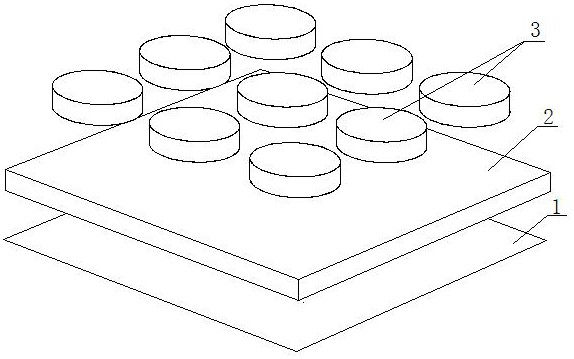
[0040] Magnetic Broadband Electromagnetic Absorbing Metamaterials, please refer to figure 1 , the electromagnetic wave-absorbing metamaterial includes a three-layer structure: the bottom layer is a copper film reflective layer, the middle layer is a FR-4 board dielectric layer, and the upper layer is an array layer composed of a plurality of magnetic structural units arranged in a rectangular array at intervals, Electromagnetic waves are incident in the Z direction from the top layer.
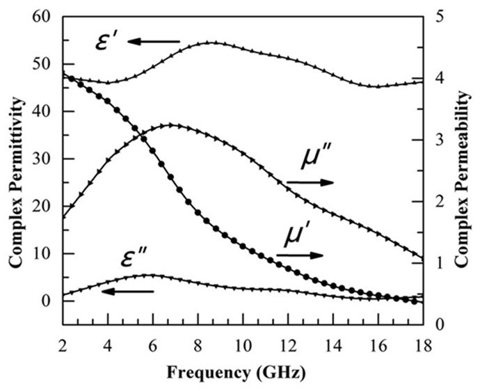
[0041] The magnetic structural unit is a mixture of FeCo alloy and adhesive, and its electromagnetic parameters are as follows figure 2 shown. The magnetic structural unit is a cylinder with a diameter of 8 mm and a height of 2 mm. The distance between two adjacent magnetic structural units in the array layer is 12 mm. The dielectric layer is an FR-4 board with a dielectric constant of 4.3, and the thickness of the dielectric layer is 2 mm. , the thickness of the copper film reflective layer...
Embodiment 2
[0048] Magnetic broadband electromagnetic wave-absorbing metamaterial, the electromagnetic wave-absorbing metamaterial includes a three-layer structure: the bottom layer is a copper film reflective layer, the middle layer is a polyester film dielectric layer, and the upper layer is a plurality of magnetic magnetic layers arranged at intervals in a rectangular array. An array layer composed of structural units, and electromagnetic waves are incident along the Z direction from the top layer.
[0049] The magnetic structural unit is a mixture of FeCo alloy and adhesive, and its electromagnetic parameters are as follows figure 2 shown. The magnetic structural unit is a cylinder with a diameter of 8 mm and a height of 2 mm. The distance between two adjacent magnetic structural units in the array layer is 12 mm. The dielectric layer is a polyester film with a dielectric constant of 3.3, and the thickness of the dielectric layer is 2 mm. The thickness of the copper film reflective ...
PUM
| Property | Measurement | Unit |
|---|---|---|
| surface roughness | aaaaa | aaaaa |
| surface roughness | aaaaa | aaaaa |
| diameter | aaaaa | aaaaa |
Abstract
Description
Claims
Application Information


