

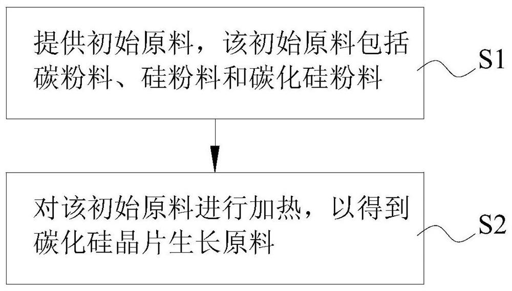
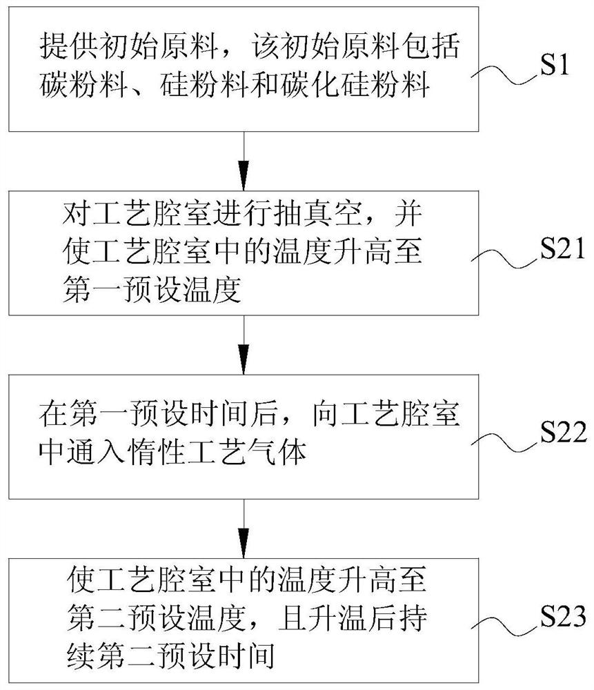
A preparation method and raw material for wafer growth
A raw material, silicon carbide wafer technology, applied in crystal growth, single crystal growth, single crystal growth and other directions, can solve the problems of easy inclusion of carbon powder, low crystal growth rate, etc., to improve productivity, good product quality, and improve particle size The effect of growth rate
- Summary
- Abstract
- Description
- Claims
- Application Information
AI Technical Summary
Problems solved by technology
Method used
Image

Examples
Embodiment Construction
[0029] The specific embodiments of the present invention will be described in detail below with reference to the accompanying drawings. It should be understood that the specific embodiments described herein are only used to illustrate and explain the present invention, but not to limit the present invention.
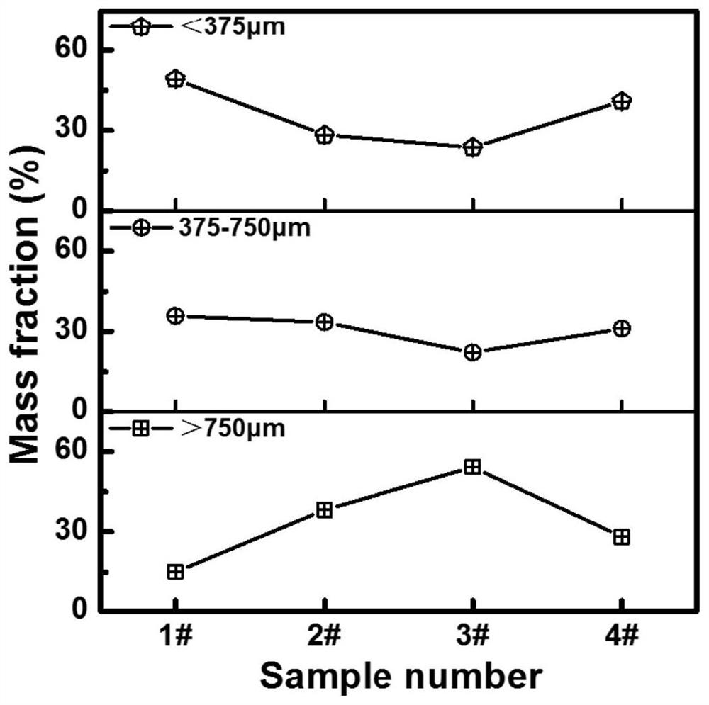
[0030] The inventors of the present invention have found after research that among various parameters of the silicon carbide raw material, the particle size is particularly important. The particle size of the silicon carbide raw material has a great influence on the gas phase composition during the growth process. The particle size of the raw material used for the growth of silicon carbide crystals is usually tens of microns to several hundreds of microns. When the number of raw material particles is large, it will not only reduce the crystal growth rate, but also easily lead to defects such as inclusion of carbon powder and other particle impurities in the crystal, whic...
PUM
| Property | Measurement | Unit |
|---|---|---|
| particle diameter | aaaaa | aaaaa |
| particle diameter | aaaaa | aaaaa |
Abstract
Description
Claims
Application Information