Narrow-band metasurface device

A metasurface, device technology, applied in instruments, optical components, optics, etc., can solve problems such as wide bandwidth, low efficiency, and filtering secondary peaks of the spectrum

Active Publication Date: 2020-09-01
SOUTHEAST UNIV
View PDF5 Cites 2 Cited by
  • Summary
  • Abstract
  • Description
  • Claims
  • Application Information

AI Technical Summary

Problems solved by technology

However, the technology of using metasurface structure for frequency selection in the visible light band is not very ma

Method used


Image

  • Narrow-band metasurface device
  • Narrow-band metasurface device
  • Narrow-band metasurface device

Examples


Embodiment 1

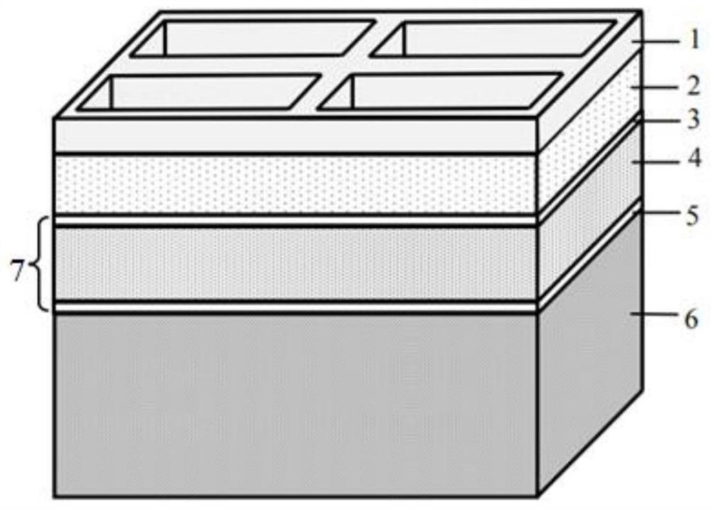
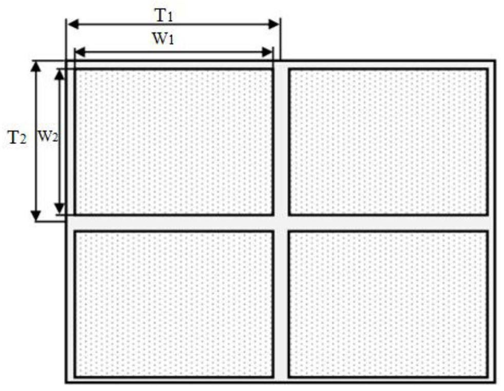
[0035] The structure of the narrow-band metasurface device in this embodiment is as figure 1 with figure 2 Shown. The two-dimensional top view of the metasurface element and the metal groove element in the groove antenna metasurface layer 1 are both square, namely T 1 = T 2 , W 1 =W 2 . The material of the supersurface layer of the groove antenna is Ag, and the period is T 1 = T 2 =340nm, W 1 =W 2 =306nm, the aperture ratio at this time is 0.81, and the thickness of the groove antenna supersurface layer 1 is 80nm. The thickness of the buffer medium layer 2 is 60 nm, and the material is magnesium fluoride. The thickness of the first transparent electrode layer 3 and the second transparent electrode layer 5 is 5nm, and the material is In 2 O 3 -SnO 2 . The thickness of the adjustable dielectric layer 4 is 120 nm, and the material is organic crystal DAST. The material of the base layer 6 is SiO 2 , The thickness is 300nm. In this embodiment, the refractive index of the adjust...

Embodiment 2

[0037] The structure of the narrow-band metasurface device in this embodiment is as figure 1 with figure 2 Shown. The two-dimensional top view of the metasurface element and the metal groove element in the groove antenna metasurface layer 1 are both square, namely T 1 = T 2 , W 1 =W 2 . The material of the supersurface layer of the groove antenna is Ag, and the period is T 1 = T 2 =340nm, W 1 =W 2 =306nm, the aperture ratio at this time is 0.81, and the thickness of the groove antenna supersurface layer 1 is 80nm. The thickness of the buffer medium layer 2 is 60 nm, and the material is magnesium fluoride. The thickness of the transparent electrode layer is 5nm, and the material is In 2 O 3 -SnO 2 . The thickness of the adjustable dielectric layer 4 is 120 nm, and the material is organic crystal DAST. The material of the base layer 6 is SiO 2 , The thickness is 300nm. In this embodiment, a voltage is applied to the transparent electrode layer, and the refractive index of th...


PUM

PropertyMeasurementUnit
Fwhmaaaaaaaaaa
Thicknessaaaaaaaaaa
Thicknessaaaaaaaaaa

Abstract

The invention discloses a narrow-band metasurface device, and the device comprises a groove antenna metasurface layer, a buffer dielectric layer, an adjustable dielectric layer group and a substrate layer which are sequentially arranged from top to bottom. The adjustable dielectric layer group comprises an adjustable dielectric layer and transparent electrode layers arranged on the upper surface and the lower surface of the adjustable dielectric layer; the groove antenna metasurface layer comprises a groove antenna metasurface structure; the groove antenna metasurface structure comprises metasurface antenna units which are periodically distributed, grooves are formed in the metasurface antenna units, and the aperture opening ratio of the metasurface antenna units is made to be greater than0.7. The refractive index of the buffer dielectric layer and the refractive index of the substrate layer are less than the refractive index of the adjustable dielectric layer. The reflectivity curveof the device provided by the invention has an extremely narrow bandwidth, and the full width at half maximum of the reflection peak is within 2nm; meanwhile, the change of the adjustable dielectric layer in the structure can change the resonance wavelength of a reflectivity curve, so the reflectivity curve can change in a visible light range or a larger range, ultrahigh efficiency and extremely narrow bandwidth are kept, and the structure can be applied to the fields of spectrum detection, spectrum inspection and the like.

Description

Technical field [0001] The invention relates to a super-surface device, in particular to a narrow-band super-surface device. Background technique [0002] The metasurface is a planar array composed of periodically arranged resonant sub-wavelength elements. By introducing phase mutations, it can get rid of the dependence on propagation effects and gain new degrees of freedom in shaping the wavefront and optical design. Compared with metamaterials usually composed of complex three-dimensional artificial nanostructures, metasurfaces have higher electromagnetic properties and have the advantage of occupying less physical space, thereby providing less structural loss. Therefore, metasurfaces are due to their flat surfaces. The profile is expected to have better advantages in the design of optical devices. [0003] At present, the working wavebands of metasurface devices are mainly in the microwave wave band and the terahertz wave band, and relatively few work in the visible light wave ...

Claims


Application Information

Patent Timeline
IPC IPC(8): G02F1/01G02B5/00
CPCG02F1/0102G02B5/008
Inventor 杨兰兰陈勇城屠彦王莉莉仲雪飞张宇宁
Owner SOUTHEAST UNIV
Why Eureka
Try Eureka