Chip packaging structure and method

A chip packaging structure and chip packaging technology, which is applied in the direction of semiconductor/solid-state device parts, semiconductor devices, electrical components, etc., can solve the problems of large volume, low integration, and large warping of the chip packaging structure, and improve the use of various performance, improve integration, and improve the effect of heat dissipation performance

Active Publication Date: 2020-09-01
NAT CENT FOR ADVANCED PACKAGING
View PDF13 Cites 5 Cited by
  • Summary
  • Abstract
  • Description
  • Claims
  • Application Information

AI Technical Summary

Problems solved by technology

[0005] In view of this, the embodiment of the present invention provides a chip packaging structure and method to solve the problems of large volume, low integration and large warpage in the existing chip packaging structure

Method used


Image

  • Chip packaging structure and method
  • Chip packaging structure and method
  • Chip packaging structure and method

Examples


Embodiment Construction

[0043] In order to make the purpose, technical solutions and advantages of the embodiments of the present invention clearer, the technical solutions in the embodiments of the present invention will be clearly and completely described below in conjunction with the drawings in the embodiments of the present invention. Obviously, the described embodiments It is a part of embodiments of the present invention, but not all embodiments. Based on the embodiments of the present invention, all other embodiments obtained by those skilled in the art without creative efforts fall within the protection scope of the present invention.

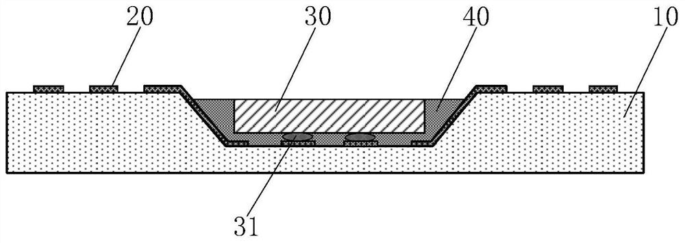
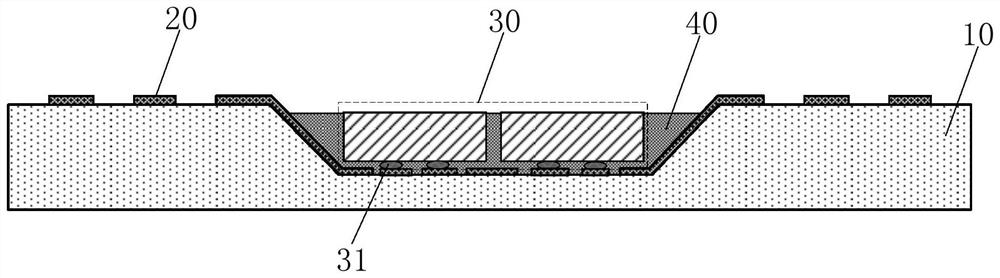
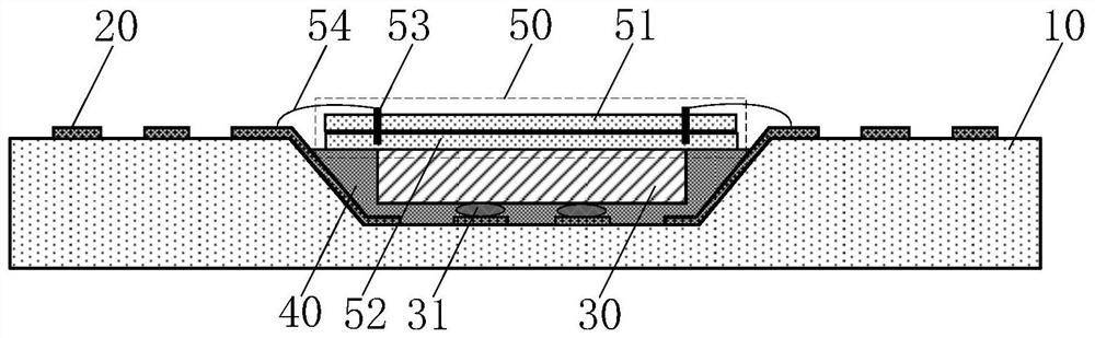
[0044] According to the first aspect, an embodiment of the present invention provides a chip packaging structure, such as figure 1 As shown, the chip package structure includes: a substrate 10, which has an accommodating space; a redistribution layer 20, arranged on the accommodating space and the surface of the substrate 10; a first chip unit 30, arranged in...


PUM


Abstract

The invention relates to the technical field of semiconductors, and particularly relates to a chip packaging structure and method. The structure comprises a substrate, a rewiring layer, a first chip unit and a first packaging layer, wherein the substrate is provided with an accommodating space; the rewiring layer is arranged in the accommodating space and on the surface of the substrate; the firstchip unit is arranged on the rewiring layer in the accommodating space and is provided with a first conductive connection point; the first conductive connection point is connected with the rewiring layer; and the first packaging layer fills the accommodating space. According to the chip packaging structure provided by the invention, the rewiring layer is arranged in the accommodating space of thesubstrate and on the surface of the substrate, and the first chip units are arranged in the accommodating space and connected with the rewiring layer, so that the space size of the packaging structure is saved, the integration degree is improved, the accommodating space is filled with the first packaging layer, the first chip unit is packaged, and the problem of large warping is avoided.

Description

technical field [0001] The invention relates to the technical field of semiconductors, in particular to a chip packaging structure and method. Background technique [0002] When packaging the first chip unit and the second chip unit chip, the current more traditional solutions include: placing the first chip unit and the second chip unit on one side of the packaging substrate, or placing the first chip unit and the second chip unit on both sides of the packaging substrate respectively. A chip unit and a second chip unit. [0003] In these two solutions, the first chip unit and the second chip unit are completely plastic-sealed with a plastic sealing layer, and when packaged, a large amount of plastic sealing material needs to be used in the packaging process, which is not conducive to the heat dissipation of the package structure, and is also prone to relatively high heat dissipation. Large warping problem leads to low product yield; and both the first chip unit and the sec...

Claims


Application Information

Patent Timeline
Patent Type & Authority Applications(China)
IPC IPC(8): H01L23/13H01L23/31H01L23/367H01L23/488H01L21/50H01L21/56H01L25/065H01L21/98
CPCH01L23/13H01L23/3157H01L23/367H01L23/488H01L21/50H01L21/56H01L25/0657H01L25/50H01L24/02H01L2225/0651H01L2225/06517H01L2225/06589H01L2224/02373H01L2224/0231H01L2224/48145H01L2924/15156H01L2224/73265H01L2224/48091H01L2224/16225H01L2224/73253H01L2924/15311H01L2924/00014
Inventor 张凯曹立强
Owner NAT CENT FOR ADVANCED PACKAGING
Why Eureka
Try Eureka