
Semiconductor layered device with data bus inversion

A data bus, bus technology, applied in the direction of electrical digital data processing, transistors, digital memory information, etc., can solve long-term problems

Pending Publication Date: 2020-09-15
MICRON TECH INC
View PDF3 Cites 0 Cited by
  • Summary
  • Abstract
  • Description
  • Claims
  • Application Information

AI Technical Summary

Problems solved by technology

The DBI calculation should be performed within 1 cycle of the read clock signal READ; however, it takes a relatively long time to complete the DBI calculation because the DBI calculator 12 is composed of a large number of logic gates
Therefore, the cycle of the read clock signal READ is required to be long enough to complete the DBI calculation, and thus the data transfer speed is inhibited by the DBI operation

Method used


Image

  • Semiconductor layered device with data bus inversion
  • Semiconductor layered device with data bus inversion
  • Semiconductor layered device with data bus inversion

Examples


Embodiment Construction

[0030] Various embodiments of the present invention will be explained in detail below with reference to the accompanying drawings. The following detailed description refers to the accompanying drawings, which show by way of illustration certain aspects and embodiments in which the invention may be practiced. This description provides sufficient detail to enable one skilled in the art to practice the embodiments of the invention. Other embodiments may be utilized and structural, logical, and electrical changes may be made without departing from the scope of the present invention. The various embodiments disclosed herein are not necessarily mutually exclusive, as some disclosed embodiments can be combined with one or more other disclosed embodiments to form new embodiments.

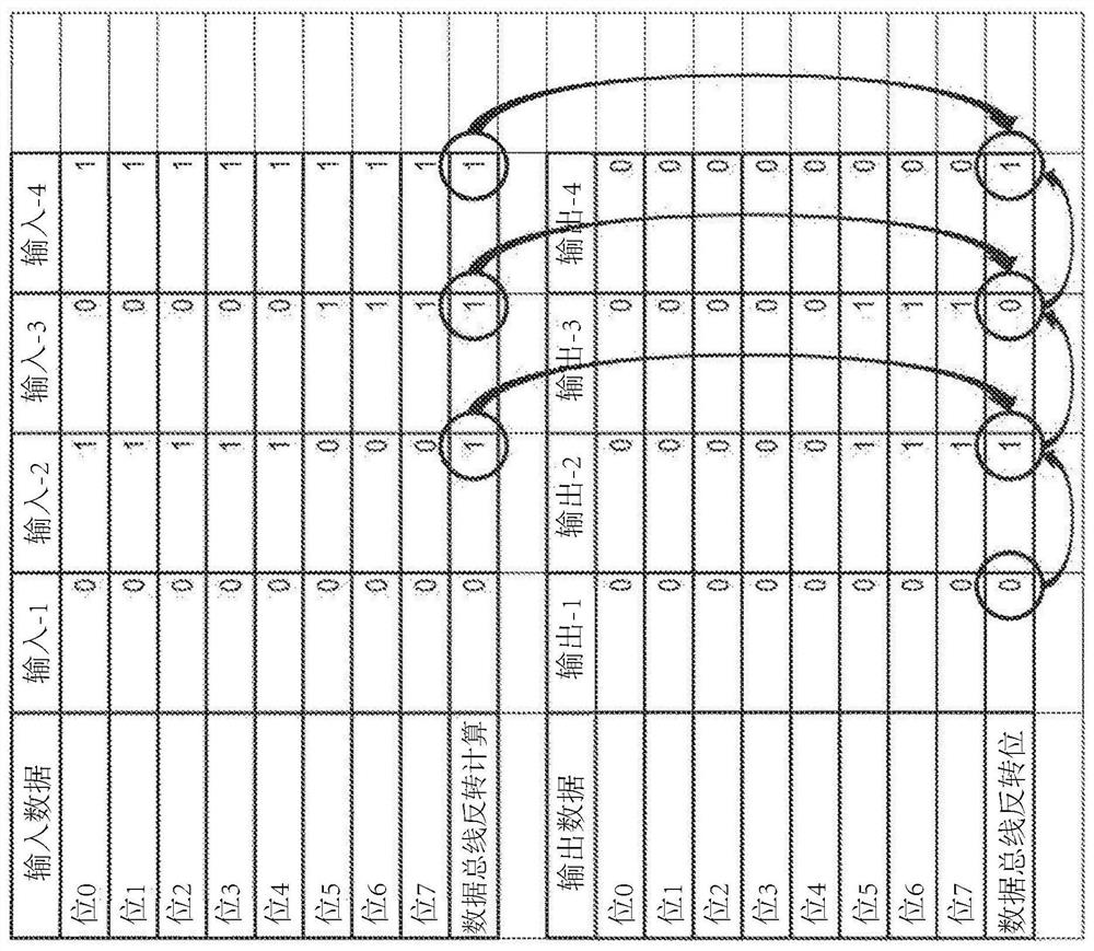
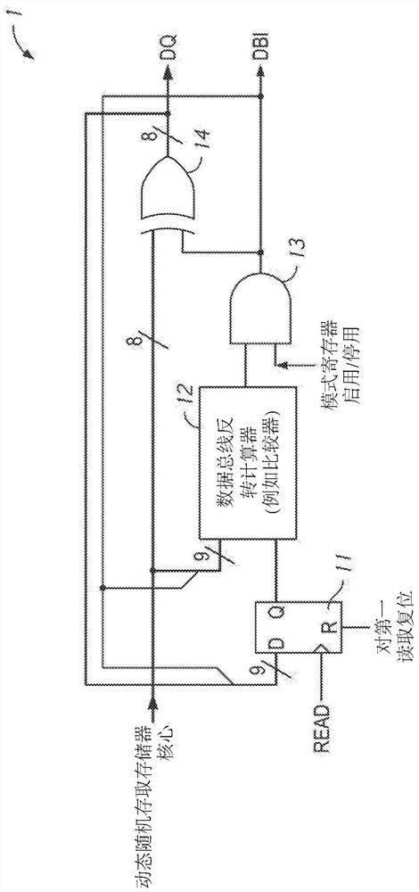
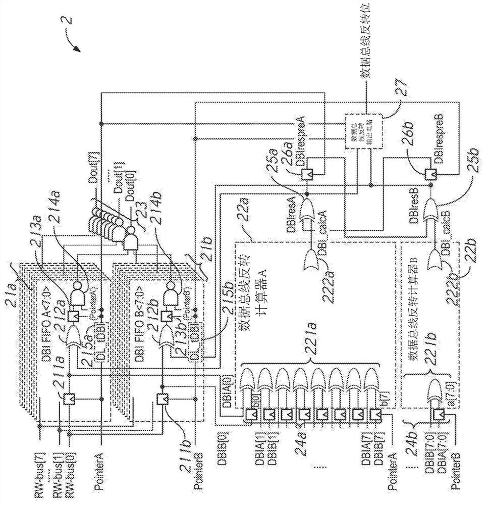
[0031] Figure 2A is a schematic diagram of a DBI circuit 2 according to an embodiment of the present invention. Figure 2B is a timing diagram of signals in the DBI circuit 2 during a DBI operation accor...


PUM


Abstract

Apparatuses and methods of data transmission between semiconductor chips are described. An example apparatus includes: a data bus inversion (DBI) circuit that receives first, second and third input data in order, and further provides first, second and third output data, either with or without data bus inversion. The DBI circuit includes a first circuit that latches the first input data and the third input data; a second circuit that latches the second input data; a first DBI calculator circuit that performs first DBI calculation on the latched first input data and the latched second input dataresponsive to the first circuit latching the first input data and the second circuit latching the second input data, respectively; and a second DBI calculator circuit that performs second DBI calculation on the latched second data and the latched third input data responsive to the first circuit latching the third input data.

Description

Background technique [0001] High data reliability, high-speed memory access, low power consumption, and reduced chip size are required features of semiconductor memories. In recent years, three-dimensional (3D) memory devices have been introduced. Some 3D memory devices are formed by stacking chips (eg, dies) vertically and interconnecting the chips using through-substrate vias (TSVs). Benefits of 3D memory devices include shorter interconnects (which reduce circuit delay and power consumption), a large number of vertical vias between layers (which allow wide bandwidth buses between functional blocks in different layers), and relatively small footprints. Thus, 3D memory devices enable higher memory access speeds, lower power consumption, and reduced chip size. Example 3D memory devices include hybrid memory cubes (HMC), high bandwidth memory (HBM), and wide I / O dynamic random access memory (DRAM). [0002] For example, high-bandwidth memory (HBM) is a type of memory that in...

Claims


Application Information

Patent Timeline
IPC IPC(8): G11C7/10
CPCG11C11/4093G11C11/4096G11C7/1006G06F13/4265H10B12/01G11C5/04Y02D10/00G11C11/4023H10B12/00
Inventor 惠比原雪成井聖司
Owner MICRON TECH INC
Learn More