Flexible Micro-LED display panel and manufacturing method thereof
A display panel and manufacturing method technology, applied to semiconductor devices, electrical components, circuits, etc., can solve the problems of display panels that are not easy to bend, easy to break, and low product yield, so as to broaden the application range and reduce disconnection Effects of Risk, High Response Speed
- Summary
- Abstract
- Description
- Claims
- Application Information
AI Technical Summary
Problems solved by technology
Method used
Image

Examples
Embodiment Construction
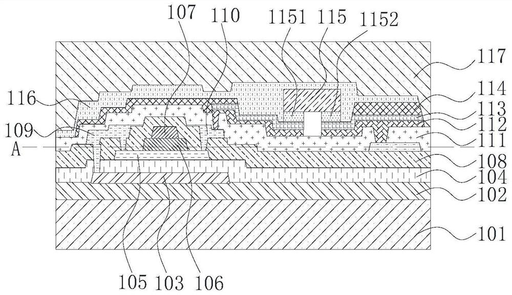
[0046] The following descriptions of the various embodiments refer to the accompanying drawings to illustrate specific embodiments in which the invention may be practiced. The directional terms mentioned in the present invention, such as [top], [bottom], [front], [back], [left], [right], [inside], [outside], [side], etc., are only for reference The orientation of the attached schema. Therefore, the directional terms used are used to illustrate and understand the present invention, but not to limit the present invention. In the figures, structurally similar elements are denoted by the same reference numerals.
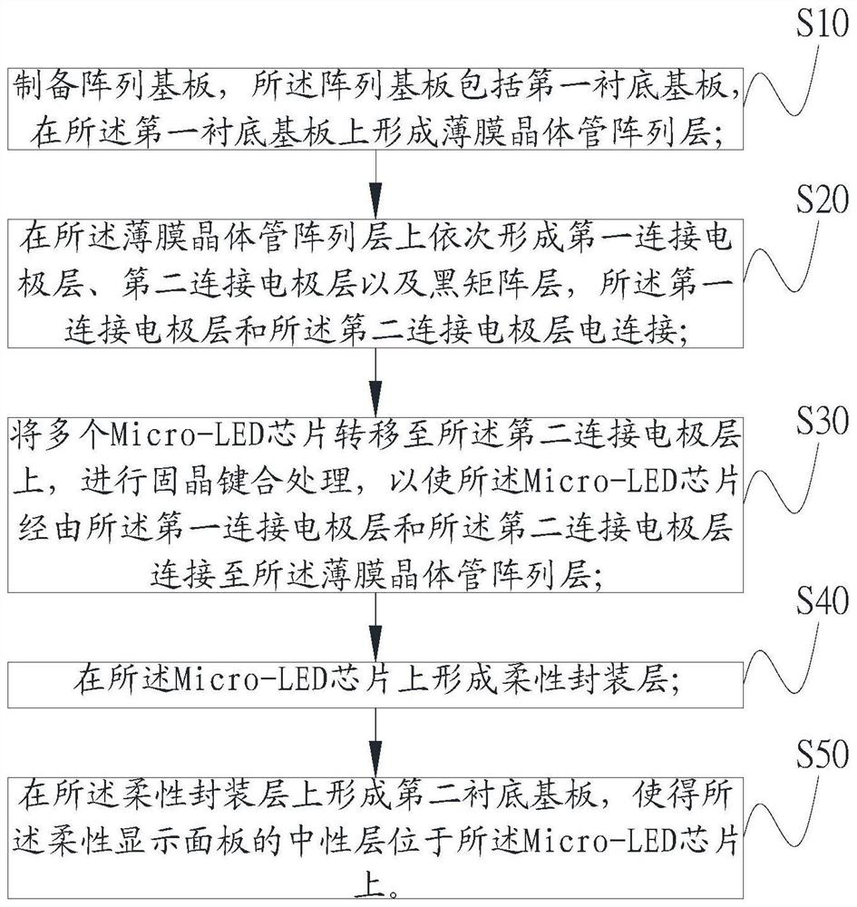
[0047] The present invention aims at the flexible Micro-LED display panel in the prior art that is not easy to bend and is prone to disconnection, resulting in low product yield, and this embodiment can solve this defect.
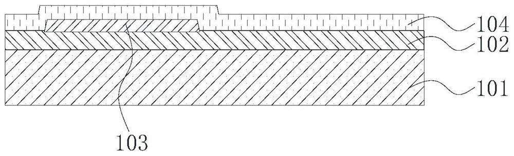
[0048] Such as figure 1 As shown, the flexible Micro-LED display panel provided by the embodiment of the present invention includes an array subst...
PUM
| Property | Measurement | Unit |
|---|---|---|
| Thickness | aaaaa | aaaaa |
Abstract
Description
Claims
Application Information