Semiconductor element sorting and testing all-in-one machine

A semiconductor and all-in-one machine technology, applied in the field of semiconductor component sorting and testing all-in-one machines, can solve problems such as low work efficiency, small number of tests, slow installation speed of semiconductor components, etc., achieve high work efficiency, fast installation speed, and improve work efficiency Effect

Inactive Publication Date: 2020-09-29
安徽富信半导体科技有限公司
View PDF6 Cites 4 Cited by
  • Summary
  • Abstract
  • Description
  • Claims
  • Application Information

AI Technical Summary

Problems solved by technology

[0003] The purpose of the present invention is to provide an integrated machine for sorting and testing semiconductor components, which solves the problem that the existing integrated machine for sorting and testing semiconductor components has a small number of single tests, cannot adjust the angle of semiconductor components, and the installation speed of semiconductor components is slow. low technical issues

Method used


Image

  • Semiconductor element sorting and testing all-in-one machine
  • Semiconductor element sorting and testing all-in-one machine
  • Semiconductor element sorting and testing all-in-one machine

Examples


Embodiment Construction

[0028] The technical solutions of the present invention will be clearly and completely described below in conjunction with the embodiments. Apparently, the described embodiments are only some of the embodiments of the present invention, not all of them. Based on the embodiments of the present invention, all other embodiments obtained by persons of ordinary skill in the art without creative efforts fall within the protection scope of the present invention.

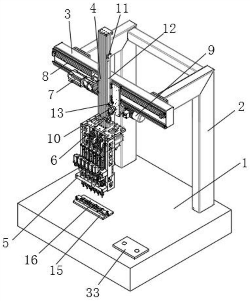
[0029] Such as Figure 1-4 As shown, a sorting and testing all-in-one machine for semiconductor components includes a base 1, a support frame 2 is fixedly installed on the upper surface of the base 1, and a crossbeam 3 is fixedly installed on the top of the support frame 2 by bolts. The crossbeam 3 One side of the moving plate 6 is movably installed, and one side of the moving plate 6 is movably installed with a lifting arm 4 along the vertical direction, and the bottom end of the lifting arm 4 is fixedly equipped with a gr...


PUM


Abstract

The invention discloses a semiconductor element sorting and testing all-in-one machine. The semiconductor element sorting and testing all-in-one machine comprises a base, wherein a supporting frame isfixedly mounted on the upper surface of the base; a transverse beam is fixedly mounted at the top of the supporting frame through a bolt; a movable plate is movably mounted at one side of the transverse beam; a hoisting arm is movably mounted at one side of the movable plate; a grasping mechanism is fixedly mounted at the bottom end of the hoisting arm; a socket plate is mounted on the upper surface of the base; a testing socket is mounted on the socket plate; a plurality of mounting grooves are formed in the testing socket; the grasping mechanism comprises a mounting plate; a plurality of outer splines are rotatably mounted on a supporting seat I; a ventilation pipe is movably mounted at the inner sides of the outer splines along the vertical direction; and a suction nozzle is fixedly mounted at the bottom of the ventilation pipe. The semiconductor element sorting and testing all-in-one machine disclosed by the invention can be used for testing a plurality of semiconductor elements in one time and the working efficiency is high; and angles of the semiconductor elements are convenient to adjust so that the semiconductor elements are accurately put into the mounting grooves and themounting speed of the semiconductor elements is rapid.

Description

technical field [0001] The invention relates to the technical field of semiconductor production equipment, in particular to an integrated machine for sorting and testing semiconductor components. Background technique [0002] The patent document (CN104096684B) discloses a sorting machine for testing semiconductor components. When the sorting machine transports the semiconductor components during the test, the angle of the semiconductor components cannot be adjusted, and manual adjustment is required. The installation accuracy is poor and the speed is slow. As a result, work efficiency is reduced. Contents of the invention [0003] The purpose of the present invention is to provide an integrated machine for sorting and testing semiconductor components, which solves the problem that the existing integrated machine for sorting and testing semiconductor components has a small number of single tests, cannot adjust the angle of semiconductor components, and the installation spee...

Claims


Application Information

Patent Timeline
Patent Type & Authority Applications(China)
IPC IPC(8): B07C5/02B07C5/344B07C5/36
CPCB07C5/02B07C5/344B07C5/362B07C2301/0008B07C2501/0063
Inventor 蒋振荣周海生
Owner 安徽富信半导体科技有限公司
Why Eureka
Try Eureka