Analog-to-digital converter based on thin film transistor, chip and control method

A technology of thin film transistors and analog-to-digital converters, which is applied in the fields of analog-to-digital converters, analog-to-digital conversions, and code conversions, and can solve the problems of low resolution of analog-to-digital converters, poor performance of analog-to-digital converters, and narrow output swings and other issues to achieve the effect of improving resolution, reducing differential nonlinear error, and improving performance

Active Publication Date: 2020-10-16
SOUTH CHINA UNIV OF TECH
View PDF4 Cites 2 Cited by
  • Summary
  • Abstract
  • Description
  • Claims
  • Application Information

AI Technical Summary

Problems solved by technology

However, limited by the development of process manufacturing level, the current process level can only manufacture unipolar n-type TFT devices, and the lack of complementary device p-type TFTs makes the inverting phase in the existing MO-TFT analog-to-digital converters The converter is usually designed based on the traditional diode load structure, resulting in poor DC gain and narrow output swing, which ultimately leads to low resolution, low accuracy, and poor performance of the ADC

Method used


Image

  • Analog-to-digital converter based on thin film transistor, chip and control method
  • Analog-to-digital converter based on thin film transistor, chip and control method
  • Analog-to-digital converter based on thin film transistor, chip and control method

Examples


Embodiment Construction

[0042] In order to enable those skilled in the art to better understand the solution of the present application, the technical solution in the embodiment of the application will be clearly and completely described below in conjunction with the accompanying drawings in the embodiment of the application. Obviously, the described embodiment is only It is an embodiment of a part of the application, but not all of the embodiments. Based on the embodiments in this application, all other embodiments obtained by persons of ordinary skill in the art without creative efforts shall fall within the scope of protection of this application.

[0043] The terms "first", "second", "third" and "fourth" in the specification and claims of the present application and the drawings are used to distinguish different objects, rather than to describe a specific order . Furthermore, the terms "include" and "have", as well as any variations thereof, are intended to cover a non-exclusive inclusion. For ...


PUM


Abstract

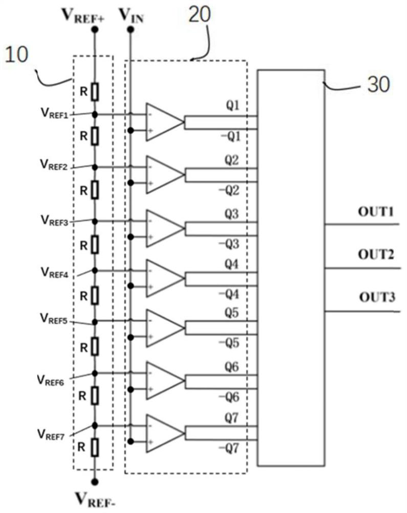
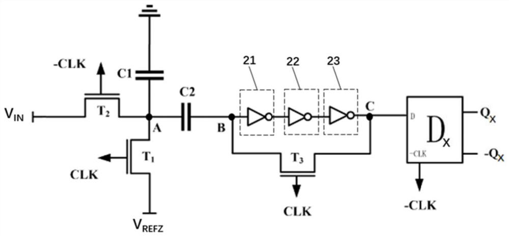
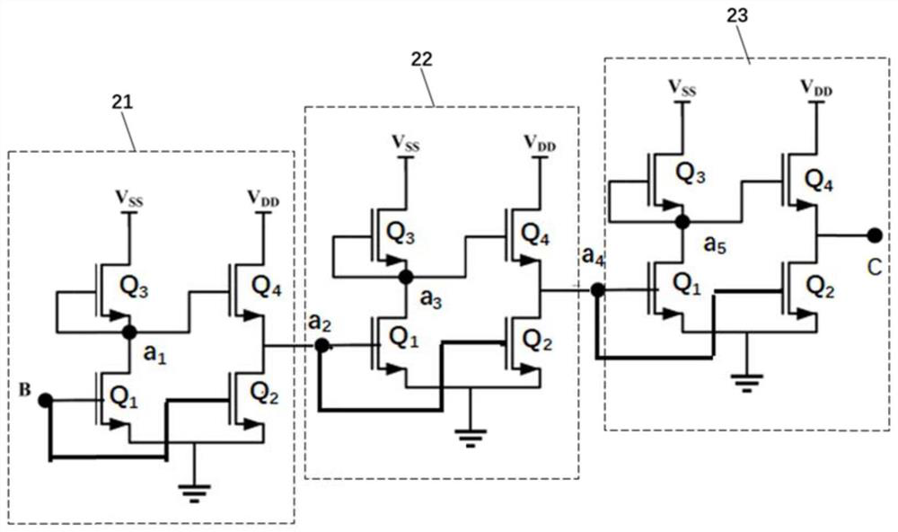
The invention discloses an analog-to-digital converter based on a thin film transistor, a chip and a control method. A reference voltage is provided for a comparator module through a reference level module, a comparison unit compares the reference voltage with an analog signal input quantity to output a first comparison quantity, then a pseudo CMOS inverter unit processes the first comparison quantity to obtain a second comparison quantity, and a decoder module decodes the second comparison quantity to obtain an output digital quantity; the pseudo CMOS inverter unit is arranged to process thefirst comparison quantity; the output swing and the direct current gain of the circuit are increased by utilizing the characteristic that the pseudo CMOS inverter unit has a shaping effect on the waveform; and due to the improvement of the direct current gain, the obtained second comparison quantity is a value obtained by further amplifying the first comparison quantity, so that the overall resolution of the comparator module can be improved, and the differential nonlinear error and the integral nonlinear error of the analog-to-digital converter are reduced. The analog-to-digital converter canbe widely applied to the technical field of integrated circuits.

Description

technical field [0001] The invention relates to the field of integrated circuits, in particular to an analog-to-digital converter based on thin film transistors, a chip and a control method. Background technique [0002] Analog-to-digital converters are important components in integrated circuits, used to convert analog signals into digital signals, and are widely used. Metal oxide thin film transistor (Meta oxide thin film transistor, MO-TFT) has the advantages of low manufacturing cost, good light transmission performance, large-area manufacturing and flexible substrate. The analog-to-digital converter based on MO-TFT has potential application prospects in the temperature measurement of electronic thermometers, digital cameras, humidity, light, sound in the air, and detection of analog signals such as biomedical electrical signals. However, limited by the development of process manufacturing level, the current process level can only manufacture unipolar n-type TFT devices...

Claims


Application Information

Patent Timeline
Patent Type & Authority Applications(China)
IPC IPC(8): H03M1/34H03M1/12
CPCH03M1/1245H03M1/34
Inventor 范厚波陈荣盛徐煜明吴朝晖李斌李国元
Owner SOUTH CHINA UNIV OF TECH
Why Eureka
Try Eureka