Storage packaging chip and pin multiplexing method thereof

A technology for storing chips and installing chips, which is applied in the direction of electrical components, electric solid devices, circuits, etc., and can solve problems such as two chips cannot be effectively synchronized, control logic is chaotic, and the functions of Flash chips are limited.

Active Publication Date: 2020-10-23
WUHAN XINXIN SEMICON MFG CO LTD
View PDF5 Cites 3 Cited by
  • Summary
  • Abstract
  • Description
  • Claims
  • Application Information

AI Technical Summary

Problems solved by technology

This sharing of a large number of pins limits the data input / output rate and the diversification of chip functions
And the Flash chip supports the serial peripheral interface (Serial Peripheral Interface, referred to as SPI) mode of the unit and the multi-bit quad peripheral interface (Quad Peripheral Interface, referred to as QPI) mode, but the RPMC chip only supports the SPI mode
In the prior art, when the Flash chip and the RPMC chip are stacked and sealed together, because the Flash chip and the RPMC chip cannot maintain exactly the same state, that is, the two chips cannot be effectively synchronized; therefore, the packaged chip only supports the SPI mode, which limits The function of the Flash chip
If the QPI function of the Flash chip is forcibly enabled, the RPMC chip is still in the SPI mode at this time. Since the Flash chip and the RPMC chip share a large number of pins, the signals received by the two chips are consistent but the working modes are different, which may easily lead to control logic failure. confusion

Method used


Image

  • Storage packaging chip and pin multiplexing method thereof
  • Storage packaging chip and pin multiplexing method thereof
  • Storage packaging chip and pin multiplexing method thereof

Examples


Embodiment Construction

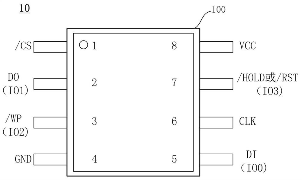
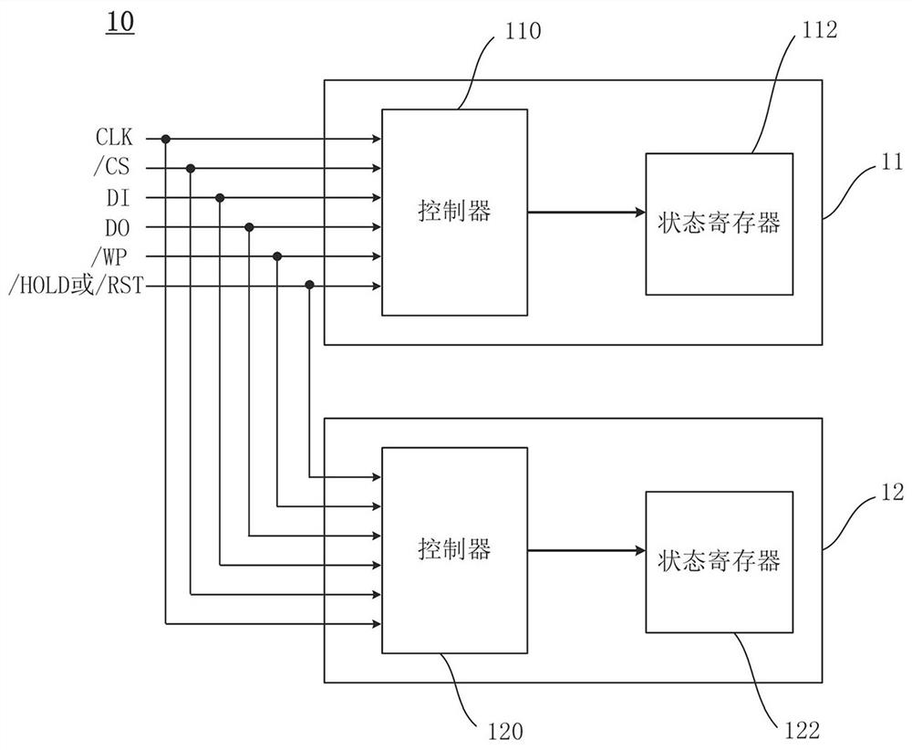
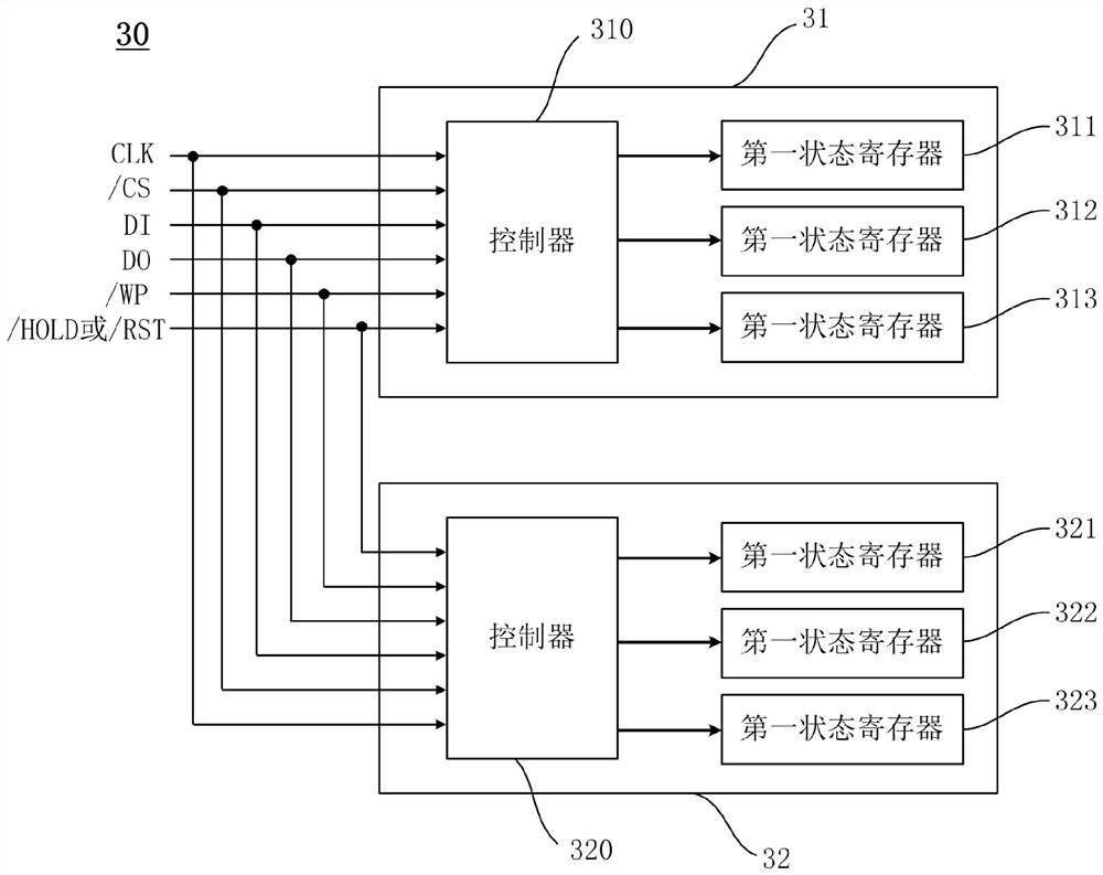
[0017] Embodiments of the present application are described in detail below, examples of which are shown in the drawings, wherein the same or similar reference numerals denote the same or similar elements or elements having the same or similar functions throughout. The embodiments described below by referring to the drawings are exemplary, are only used to explain the present application, and cannot be construed as limiting the present application.

[0018] In the description of this application, it should be noted that unless otherwise specified and limited, the terms "installation", "connection" and "connection" should be understood in a broad sense, for example, it can be a fixed connection or a detachable connection, Or integrally connected; can be mechanically connected, can also be electrically connected or can communicate with each other; can be directly connected, can also be indirectly connected through an intermediary, can be the internal communication of two componen...


PUM


Abstract

The invention discloses a storage packaging chip and a pin multiplexing method thereof. The storage packaging chip comprises at least one storage chip and an expansion chip which can receive the sameexternal input signal; and by additionally arranging a state register with the state bits for setting multiplexing and function switching of the pin groups of the expansion chip in the expansion chip,the configuration of the corresponding state bits in the expansion chip can be realized, so that the expansion chip supports a QPI mode and can be synchronized with the storage chip.

Description

technical field [0001] The present application relates to the technical field of semiconductors, in particular to a storage package chip and a pin multiplexing method thereof. Background technique [0002] Memory (Memory) is a memory device in a computer system used to store programs and data. All information in the computer, including input raw data, computer programs, intermediate running results and final running results are stored in the memory. In recent years, during the rapid development of semiconductor memory, flash memory (Flash) has become a memory commonly used in computers and mobile communication terminals due to its advantages of high density, low power consumption and low price. [0003] An enhanced flash memory chip with a response protection monotonic counter (Replay Protection Monotonic Counter, RPMC for short), usually integrates the Flash chip and the RPMC chip on a bare chip. The Flash chip is used to store the code and data of the Basic Input-Output ...

Claims


Application Information

Patent Timeline
Patent Type & Authority Applications(China)
IPC IPC(8): H01L23/31
CPCH01L23/31
Inventor 卢中舟
Owner WUHAN XINXIN SEMICON MFG CO LTD
Why Eureka
Try Eureka