LED packaging process method

A technology of LED packaging and process method, which is applied in the direction of electrical components, circuits, semiconductor devices, etc., can solve the problems of poor heat dissipation effect and short service life, and achieve the effects of easy control, good durability, and improved light extraction efficiency

Pending Publication Date: 2020-10-27
苏州雷霆光电科技有限公司
View PDF3 Cites 0 Cited by
  • Summary
  • Abstract
  • Description
  • Claims
  • Application Information

AI Technical Summary

Problems solved by technology

The LED packaging is to complete the output of electrical signals, protect the normal operation of the die, and output: the function of visible light, which has both electrical parameters and optical parameters design and technical ...

Method used


Image

  • LED packaging process method

Examples


Embodiment 1

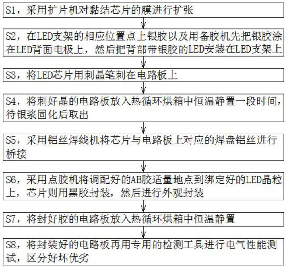
[0027] Embodiment 1: a kind of LED encapsulation process method, comprises the following steps:

[0028] S1, using the expansion machine to expand the film of the bonded chip;

[0029] S2, apply silver glue on the corresponding position of the LED bracket and apply the silver glue on the back electrode of the LED with a glue preparation machine, and then install the LED with the silver glue on the back of the LED bracket;

[0030] S3, stabbing the LED chip on the circuit board with a spine pen;

[0031] S4, put the thorned circuit board into a thermal cycle oven at a constant temperature and let it stand for a period of time, and take it out after the silver paste is solidified;

[0032] S5, using an aluminum wire bonding machine to bridge the chip with the corresponding pad aluminum wire on the circuit board;

[0033] S6, using a glue dispenser to place an appropriate amount of the prepared AB glue on the bound LED die, and the chip is packaged with black glue, and then the...

Embodiment 2

[0041] Embodiment 2, an LED encapsulation process method, includes the following steps:

[0042] S1, using the expansion machine to expand the film of the bonded chip;

[0043] S2, apply silver glue on the corresponding position of the LED bracket and apply the silver glue on the back electrode of the LED with a glue preparation machine, and then install the LED with the silver glue on the back of the LED bracket;

[0044] S3, stabbing the LED chip on the circuit board with a spine pen;

[0045] S4, put the thorned circuit board into a thermal cycle oven at a constant temperature and let it stand for a period of time, and take it out after the silver paste is solidified;

[0046] S5, using an aluminum wire bonding machine to bridge the chip with the corresponding pad aluminum wire on the circuit board;

[0047] S6, using a glue dispenser to place an appropriate amount of the prepared AB glue on the bound LED die, and the chip is packaged with black glue, and then the appeara...


PUM


Abstract

The invention relates to the technical field of LED packaging, and particularly relates to an LED packaging process method. The method comprises the steps of S1, expanding a film for bonding a chip byadopting a chip expander; S2, dispensing elargol at the corresponding position of an LED support, and coating the elargol on an LED back electrode by using a glue preparation machine; S3, pricking the LED chip on the circuit board by using a pricking pen; S4, putting the pricked circuit board into a thermal cycle oven, and standing for a period of time at a constant temperature; S5, bridging thechip with a corresponding bonding pad aluminum wire on the circuit board by adopting an aluminum wire bonding machine; S6, dispensing a proper amount of the prepared AB glue on the bound LED crystal grains by adopting a glue dispenser, packaging the chip by using black glue, and then performing appearance packaging; S7, putting the packaged circuit board into the thermal cycle oven, and standing at a constant temperature; and S8, testing the electrical performance of the packaged circuit board by using a special detection tool, and distinguishing whether the circuit board is qualified or not.According to the invention, the problems of certain flaws, poor heat dissipation effect and short service life of the traditional LED packaged product are solved.

Description

technical field [0001] The invention relates to the technical field of LED packaging, in particular to an LED packaging process method. Background technique [0002] LED packaging technology is mostly developed and evolved on the basis of discrete device packaging technology, but it has great particularity. Generally, the die of a discrete device is sealed in a package, and the function of the package is mainly to protect the die and complete electrical interconnection. The LED packaging is to complete the output of electrical signals, protect the normal operation of the die, and output: the function of visible light. It has both electrical parameters and optical parameters design and technical requirements. It is impossible to simply use the packaging of discrete devices for LEDs. [0003] In the prior art, traditional LED packaged products have certain flaws, poor heat dissipation and short service life. Contents of the invention [0004] The purpose of the present inv...

Claims


Application Information

Patent Timeline
IPC IPC(8): H01L33/00H01L33/48H01L33/54
CPCH01L33/005H01L33/48H01L33/54
Inventor 蔡志嘉
Owner 苏州雷霆光电科技有限公司
Why Eureka
Try Eureka