Supercharge Your Innovation With Domain-Expert AI Agents!

Monocrystalline silicon wafer cleaning device and process

A technology for single crystal silicon wafers and cleaning devices, applied in cleaning methods and appliances, cleaning methods using liquids, chemical instruments and methods, etc., can solve the problems that the polycrystalline cleaning process cannot be adapted to single crystal cleaning, etc.

Inactive Publication Date: 2020-10-30
江苏美科太阳能科技股份有限公司
View PDF4 Cites 2 Cited by
  • Summary
  • Abstract
  • Description
  • Claims
  • Application Information

AI Technical Summary

Problems solved by technology

[0003] The purpose of the present invention is to solve the problem that the original polycrystalline cleaning process in the prior art can no longer adapt to single crystal cleaning, and propose a single crystal silicon wafer cleaning device and process

Method used


Image

  • Monocrystalline silicon wafer cleaning device and process

Examples


Embodiment Construction

[0024] The following will clearly and completely describe the technical solutions in the embodiments of the present invention with reference to the accompanying drawings in the embodiments of the present invention. Obviously, the described embodiments are only some, not all, embodiments of the present invention.

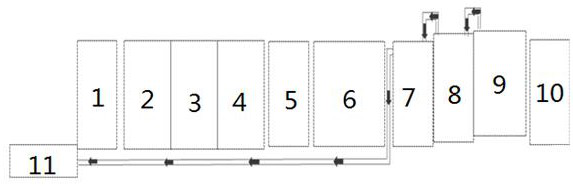
[0025] A monocrystalline silicon wafer cleaning device, including ten consecutive cleaning tanks and filter baskets for placing monocrystalline silicon wafers, the filter baskets are placed in each cleaning tank for cleaning and soaking, and the filter basket is grasped by a mechanical arm for cleaning. selective placement and removal;

[0026] The ten cleaning tanks are the first soaking tank 1, the second ultrasonic overflow tank 2, the third ultrasonic cleaning tank 3, the fourth ultrasonic cleaning tank 4, the fifth ultrasonic overflow tank 5, the sixth organic cleaning tank 6, the The seventh overflow cleaning tank 7, the eighth overflow cleaning tank 8, the nin...


PUM


Abstract

The invention belongs to the technical field of monocrystalline cleaning, and particularly relates to a monocrystalline silicon wafer cleaning device and process. The monocrystalline silicon wafer cleaning device comprises ten cleaning tanks which are continuously arranged and a filter basket used for containing monocrystalline silicon wafers, wherein the ten cleaning tanks sequentially comprise the first soaking tank, the second ultrasonic overflow tank, the third ultrasonic cleaning tank, the fourth ultrasonic cleaning tank, the fifth ultrasonic overflow tank, the sixth organic cleaning tank, the seventh overflow cleaning tank, the eighth overflow cleaning tank, the ninth overflow cleaning tank and the tenth lifting tank; cleaning liquid in the ninth overflow cleaning tank overflows to the eighth overflow cleaning tank, and cleaning liquid in the eighth overflow cleaning tank overflows to the seventh overflow cleaning tank; and the filter basket is sequentially put in and taken out of the first soaking tank, the second ultrasonic overflow tank, the third ultrasonic cleaning tank, the fourth ultrasonic cleaning tank, the fifth ultrasonic overflow tank, the sixth organic cleaning tank, the seventh overflow cleaning tank, the eighth overflow cleaning tank, the ninth overflow cleaning tank and the tenth lifting tank. In the actual production process, the monocrystalline silicon wafer cleaning device and process specially reduce the monocrystalline silicon powder dirt generation rate.

Description

technical field [0001] The invention relates to the technical field of single crystal cleaning, in particular to a single crystal silicon wafer cleaning device and process. Background technique [0002] The rapid development of monocrystalline silicon wafer production capacity has rapidly squeezed the proportion of the original polycrystalline production capacity; the subsequent original polycrystalline cleaning process can no longer adapt to the cleaning of single crystal, and the requirements for single crystal are higher and the process is more complicated. Variety diversification. Contents of the invention [0003] The object of the present invention is to solve the problem that the original polycrystalline cleaning process in the prior art cannot adapt to single crystal cleaning, and proposes a single crystal silicon wafer cleaning device and process. [0004] In order to achieve the above object, the present invention adopts the following technical solutions: [00...

Claims


Application Information

Patent Timeline
Patent Type & Authority Applications(China)
IPC IPC(8): B08B3/12B08B3/08B08B13/00
CPCB08B3/12B08B3/08B08B13/00
Inventor 杨超王艺澄
Owner 江苏美科太阳能科技股份有限公司
Features
  • R&D
  • Intellectual Property
  • Life Sciences
  • Materials
  • Tech Scout
  • Unparalleled Data Quality
  • Higher Quality Content
  • 60% Fewer Hallucinations
Learn More