Micro-LED epitaxial structure and manufacturing method thereof

A technology of epitaxial structure and epitaxial growth, which is applied in the direction of electrical components, circuits, semiconductor devices, etc., and can solve problems such as increasing carrier matching

Pending Publication Date: 2020-10-30
JIANGSU INST OF ADVANCED SEMICON CO LTD
View PDF0 Cites 3 Cited by
  • Summary
  • Abstract
  • Description
  • Claims
  • Application Information

AI Technical Summary

Problems solved by technology

In order to solve the above problems, the present invention relates to a related epitaxial structure with superlattice (SL) as the light-emitting active region, and replaces the complicated before and after with multiple quantum wells as the active region in the traditional structure with an electron deceleration layer and a hole accumulation layer. The stress release layer and electron blocking layer are designed to simplify the epitaxial growth structure, reduce the SRH non-radiative recombination and weakening polarization field effect caused by the sharp decrease in chip size and the sharp increase in defect density, and increase the carrier matching, thereby improving the new The light extraction efficiency of Micro-LED (especially below 100 micron chip size) promotes its application in display and other fields

Method used


Image

  • Micro-LED epitaxial structure and manufacturing method thereof
  • Micro-LED epitaxial structure and manufacturing method thereof
  • Micro-LED epitaxial structure and manufacturing method thereof

Examples


Embodiment Construction

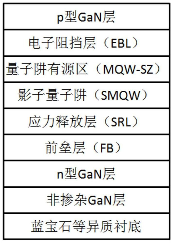
[0025] The specific implementation of the micro-LED epitaxial structure and its manufacturing method provided by the present invention will be described in detail below with reference to the accompanying drawings.

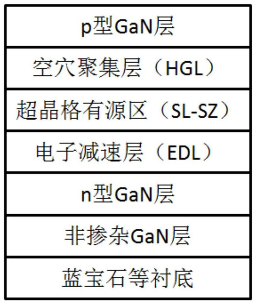
[0026] attached figure 2 Shown is a schematic diagram of the structure of the micro-LED in this specific embodiment, including a substrate layer, and an n-type semiconductor layer on the surface of the substrate, a light-emitting layer, and a p-type semiconductor layer, and the light-emitting layer includes an electron deceleration layer ( EDL), superlattice active zone (SL-SZ), and hole gathering layer (HGL).

[0027] In this specific embodiment, the substrate is a sapphire substrate, and in other specific embodiments, the substrate may also be a GaN self-supporting substrate, either polar or non-polar. The n-type semiconductor layer, the light-emitting layer, and the p-type semiconductor layer are sequentially an n-type GaN layer, a light-emitting layer, and a ...


PUM

PropertyMeasurementUnit
thicknessaaaaaaaaaa
thicknessaaaaaaaaaa
thicknessaaaaaaaaaa

Abstract

The invention provides a micro-LED epitaxial structure and a manufacturing method thereof, the micro-LED epitaxial structure comprises a substrate and also comprises an n-type semiconductor layer, a light-emitting layer and a p-type semiconductor layer which are arranged on the surface of the substrate, and the light-emitting layer comprises an electron deceleration layer, a superlattice active region and a hole aggregation layer. According to the structure, the epitaxial growth structure can be simplified, the light emitting efficiency of a micro-LED is improved, and the application of the micro-LED in the display field is promoted.

Description

technical field [0001] The invention relates to the field of light emitting diodes, in particular to a micro-LED epitaxial structure and a manufacturing method thereof. Background technique [0002] GaN-based light-emitting diodes (LEDs) are widely used because the light-emitting layer can mix narrow-bandgap InGaN materials (corresponding to long-wavelength light) and wide-bandgap AlGaN materials (corresponding to short-wavelength light), thereby achieving full-spectrum light emission. In lighting display and its related applications. With the development of technology, LED chips tend to be more and more miniaturized and integrated, and Micro-LED is born. attached figure 1 Shown is a schematic diagram of an epitaxial structure in the prior art, which is mainly composed of a substrate, an n-type region, a light-emitting active region and a p-type region. Among them, the light-emitting active region uses the multi-quantum well structure (MQW) of In(Al)GaN. By modulating the...

Claims


Application Information

Patent Timeline
Patent Type & Authority Applications(China)
IPC IPC(8): H01L33/06H01L33/12H01L33/14H01L33/32H01L33/00
CPCH01L33/0075H01L33/06H01L33/12H01L33/145H01L33/325
Inventor 王国斌王建峰徐科
Owner JIANGSU INST OF ADVANCED SEMICON CO LTD
Why Eureka
Try Eureka