Thin film transistor integrated amplifier

A technology of thin film transistors and transistors, applied in amplifiers, improved amplifiers to reduce the harmful effects of internal resistance, parts of amplifiers, etc., can solve the problems of low reliability, low bandwidth, low gain, etc., and achieve strong drive capability, The effect of increasing the amplification gain and increasing the output impedance

Pending Publication Date: 2020-10-30
PEKING UNIV SHENZHEN GRADUATE SCHOOL
View PDF0 Cites 3 Cited by
  • Summary
  • Abstract
  • Description
  • Claims
  • Application Information

AI Technical Summary

Problems solved by technology

However, the existing TFT-integrated amplifier circuits still have the technical problems of low gain, low bandwidth due to the influence of their own parasitic capacitance, and low reliability.

Method used


Image

  • Thin film transistor integrated amplifier
  • Thin film transistor integrated amplifier
  • Thin film transistor integrated amplifier

Examples


Embodiment 1

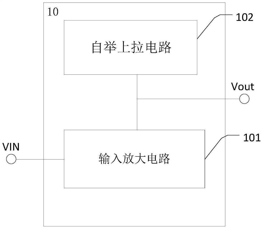
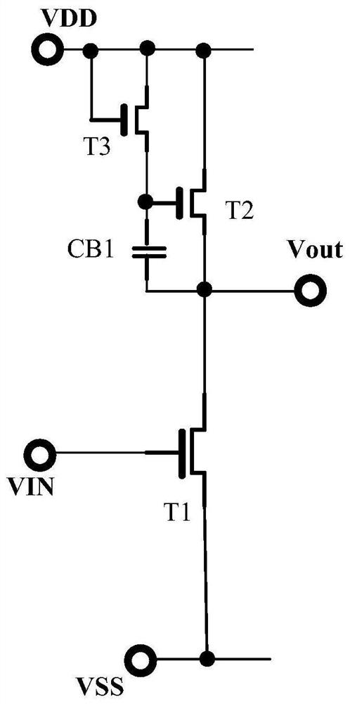
[0038] Please refer to figure 1 , figure 1 It is a structural block diagram of an amplifier integrated with thin film transistors in an embodiment. The amplifier includes a single-ended amplifier circuit unit 10 , and the single-ended amplifier circuit unit 10 includes: an input amplifier circuit 101 and a bootstrap pull-up circuit 102 .

[0039] The input amplifier circuit 101 is used for converting the signal received by its signal input terminal VIN and outputting it through the signal output terminal Vout.

[0040] The bootstrap pull-up circuit 102 is used to pull up the potential of the signal output by the signal output terminal Vout, and increase the output impedance of the bootstrap pull-up circuit 102, so as to stabilize the static operating point of the single-ended amplifying circuit unit and improve the single-ended The amplification gain of the amplifying circuit unit, the amplification gain of the single-ended amplifying circuit unit is positively related to the...

Embodiment 2

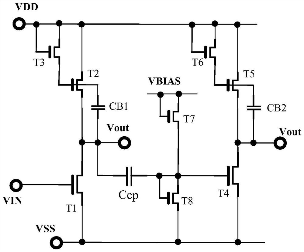
[0059] Please refer to Figure 5 , Figure 5 It is a structural block diagram of an amplifier integrated with thin film transistors in an embodiment. The amplifier includes at least one double-terminal amplifier circuit unit 20 cascaded, and the double-terminal amplifier circuit unit 20 includes: a positive-phase input circuit 201, a negative-phase input circuit 202 . A positive-phase bootstrap pull-up circuit 203 and a negative-phase bootstrap pull-up circuit 204 .

[0060] The positive-phase input circuit 201 is used for converting the positive-phase signal received by its normal-phase signal input terminal VIN_P, and outputting it through the normal-phase signal output terminal VOUT_P.

[0061] The negative-phase input circuit 202 is used for converting the negative-phase signal received by its negative-phase signal input terminal VIN_N, and outputting it through the negative-phase signal output terminal VOUT_N.

[0062] The positive-phase bootstrap pull-up circuit 203 is...


PUM


Abstract

The invention discloses a thin film transistor integrated amplifier, which comprises a single-ended amplifying circuit unit, and a bootstrap pull-up circuit, wherein the input amplifying circuit is used for imputing the amplifying circuit to amplify the signal received by the signal input end; and the bootstrap pull-up circuit is used for pulling up the potential of the signal output by the signaloutput end and increasing the output impedance of the bootstrap pull-up circuit so as to improve the amplifying gain of the single-ended amplifying circuit unit. The thin film transistor integrated amplifier also comprises a double-ended amplifying circuit unit, the positive / negative phase input circuit is used for amplifying positive / negative phase signals received by the positive / negative phasesignal input end; the positive / negative phase bootstrap pull-up circuit is used for pulling up the potential of the positive / negative phase output signal and increasing the output impedance of the positive / negative phase bootstrap pull-up circuit so as to improve the amplifying gain of the double-ended amplifying circuit unit. By improving the amplifying gains of the single-ended amplifying circuit unit and the double-ended amplifying circuit unit, the thin film transistor integrated amplifier has excellent performance.

Description

technical field [0001] The invention relates to the technical field of amplifiers, in particular to an amplifier integrated with thin film transistors, which can be applied to photoelectric sensing circuits and systems, power management circuits and systems, filter circuits and systems, temperature sensing circuits and systems of amplifiers integrated with thin film transistors. System, biomedical signal modulation and demodulation circuit, identification and modulation of radio frequency signal, etc. Background technique [0002] The rapid development of thin film transistor (thin film transistor, TFT) technology has promoted the significant progress of active display technology represented by large-size TV display and high-resolution small-size portable display. In the traditional sense, TFT is only used as a switching element of an active display array for transmission of display voltage signals. With the gradual realization of large-scale mass production of emerging dis...

Claims


Application Information

Patent Timeline
Patent Type & Authority Applications(China)
IPC IPC(8): H03F1/08
CPCH03F1/083
Inventor 张盛东廖聪维梁键安军军邱赫梓彭志超杨激文
Owner PEKING UNIV SHENZHEN GRADUATE SCHOOL
Why Eureka
Try Eureka