Automatic semiconductor chip packaging device

A chip packaging and semiconductor technology, applied in semiconductor/solid-state device manufacturing, electrical components, circuits, etc., can solve problems such as burns, operational hazards, defective products, etc., achieve reasonable structure, avoid burrs, and improve work efficiency.

Inactive Publication Date: 2020-11-10
DONGGUAN XIANGFEI INTELLIGENT EQUIP TECH CO LTD
View PDF0 Cites 14 Cited by
  • Summary
  • Abstract
  • Description
  • Claims
  • Application Information

AI Technical Summary

Problems solved by technology

[0004] Aiming at the deficiencies of the prior art, the present invention provides an automatic semiconductor chip packaging device, which solves the problem that the existing semiconductor chip packaging device proposed in the above-mentioned background technology usually requires manual loading and unloading, and sometimes the plastic packaging compound has not yet been prepared. Complete cooling, directly holding it will cause burns, so the operation has certain risks. In addition, during the plastic sealing process of semiconductor chips, sometimes there will be flashing, that is, a layer of film (commonly known as burr) will be formed on the concave part or the surface of the metal terminal. If it is not removed in time in the follow-up quality control, defective products will occur

Method used


Image

  • Automatic semiconductor chip packaging device
  • Automatic semiconductor chip packaging device
  • Automatic semiconductor chip packaging device

Examples


Embodiment Construction

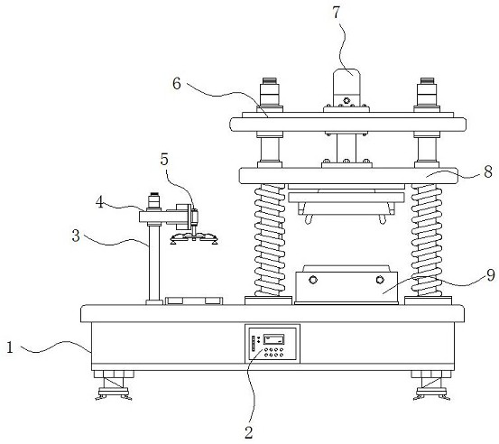
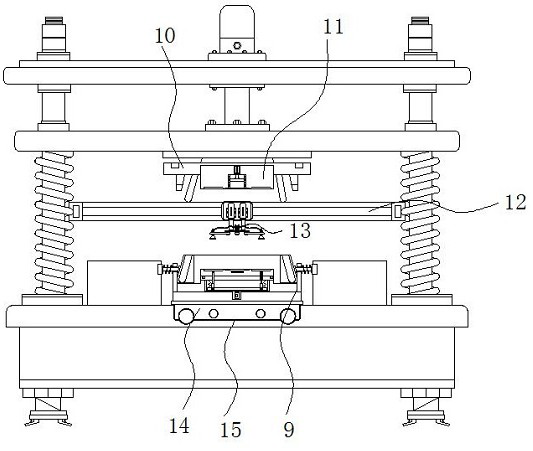
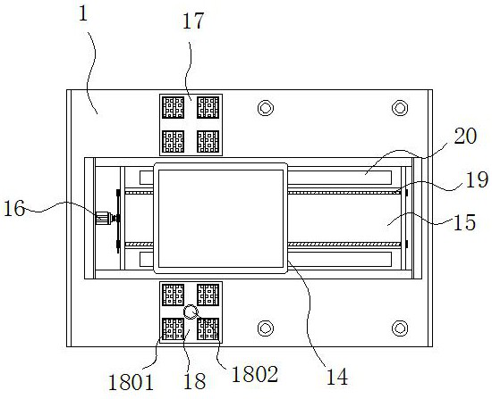
[0028] The following will clearly and completely describe the technical solutions in the embodiments of the present invention with reference to the accompanying drawings in the embodiments of the present invention. Obviously, the described embodiments are only some, not all, embodiments of the present invention.

[0029] In the description of the present invention, unless otherwise stated, the meaning of "plurality" is two or more; the terms "upper", "lower", "left", "right", "inner", "outer" , "front end", "rear end", "head", "tail", etc. indicate the orientation or positional relationship based on the orientation or positional relationship shown in the drawings, and are only for the convenience of describing the present invention and simplifying the description, rather than Indicates or implies that the device or element referred to must have a particular orientation, be constructed and operate in a particular orientation, and therefore should not be construed as limiting the...


PUM

PropertyMeasurementUnit
diameteraaaaaaaaaa

Abstract

The automatic semiconductor chip packaging device specifically comprises a base, a material taking mechanism, a lower die base, a discharging bin and a movable groove, wherein a control panel is installed in the middle of one end of the base; a frame body is installed on one side of the top of the base, and supporting columns are fixed to the two ends of the other side of the top of the base; a mounting plate is fixed to the top ends between the supporting columns, an electromagnetic sliding rail is mounted on the side, close to the frame body, of the mounting plate, a sliding block is arranged in the electromagnetic sliding rail, a material taking mechanism is mounted on the side, close to the frame body, of the sliding block, a hydraulic cylinder is mounted in the middle of the top end of the frame body, and a movable plate is arranged on the frame body below the hydraulic cylinder. According to the automatic semiconductor chip packaging device, through the arrangement of the material taking mechanism, the device can achieve automatic feeding and discharging, the situation that workers are scalded due to the fact that the workers take out the semiconductor chips manually is avoided, the time for waiting for cooling originally is saved, and the working efficiency is greatly improved.

Description

technical field [0001] The invention relates to the technical field of chip packaging, in particular to an automatic semiconductor chip packaging device. Background technique [0002] Epoxy molding compound is a powder molding compound made of epoxy resin as the matrix resin, high-performance phenolic resin as the curing agent, silicon micropowder as the filler, and various additives. The necessary material for encapsulation, the plastic encapsulation process is to use the transfer molding method to extrude the molten epoxy molding compound into the mold cavity, embed the semiconductor chip in it, and cross-link and solidify at the same time to form a semiconductor device with a certain structural appearance , In addition to protecting the chip from external dust, moisture, ions, radiation, and mechanical impact, the packaging material also plays the role of mechanical support and heat dissipation. [0003] Existing semiconductor chip packaging devices usually require manua...

Claims


Application Information

Patent Timeline
Patent Type & Authority Applications(China)
IPC IPC(8): H01L21/67B29C45/02B29C45/14B29C45/17
CPCB29C45/02B29C45/14B29C45/14008B29C45/17H01L21/67126
Inventor 邓珊林镇炜王龙
Owner DONGGUAN XIANGFEI INTELLIGENT EQUIP TECH CO LTD
Why Eureka
Try Eureka