Physical information hiding structure based on structural unit size difference and preparation method thereof
A structural unit and information hiding technology, applied in the field of information hiding, can solve the problems of small hidden information capacity and low security, and achieve the effects of high privacy and security, high information capacity, and large hidden information capacity
- Summary
- Abstract
- Description
- Claims
- Application Information
AI Technical Summary
Problems solved by technology
Method used
Image
Examples
Embodiment 1
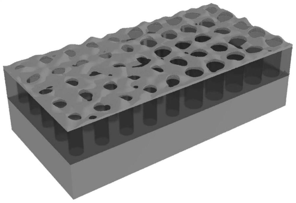
[0053] This embodiment provides a physical information hiding structure based on the size difference of structural units, which includes a substrate and a metal reflective layer stacked from bottom to top, and several structural units are arranged on the metal reflective layer. Such as figure 1 As shown, the structural unit includes a dielectric layer disposed on the metal reflective layer and a semi-continuous film of metal particles covering the upper surface of the dielectric layer; as figure 1 As shown, each structural unit is provided with a hole penetrating through the dielectric layer and the semi-continuous film of metal particles along the direction perpendicular to the metal reflective layer. The pore diameter of a hole is defined as the characteristic size of the structural unit to which the hole belongs. The shapes of any two structural units are the same, and in this embodiment, the radial section of the hole is a circle.
[0054] The substrate may be a silicon ...
Embodiment 2
[0066] This embodiment provides the preparation method of the physical information hiding structure based on the size difference of the structural units of the embodiment 1, including the following steps:
[0067] S1. Clean the substrate: clean the silicon wafer, use acetone to 2 Submerge the silicon wafer, place the whole in an ultrasonic cleaning machine and ultrasonically clean it for 5 minutes, then replace the acetone with isopropanol and then ultrasonically clean it for 5 minutes, then replace the isopropanol with water and ultrasonically clean it for 5 minutes, and finally clean the silicon wafer Take it out, and dry its surface with a nitrogen gun.
[0068] S2. Preparing the metal reflective layer: that is, evaporating an aluminum film, and evaporating an aluminum film with a thickness of 100 nm on the cleaned silicon wafer with thermal evaporation equipment.
[0069] S3. Spin-coating electron beam glue: Spin-coat a layer of ZEP electron glue with a thickness of about...
PUM
| Property | Measurement | Unit |
|---|---|---|
| thickness | aaaaa | aaaaa |
| thickness | aaaaa | aaaaa |
| thickness | aaaaa | aaaaa |
Abstract
Description
Claims
Application Information
 - R&D
- Intellectual Property
- Life Sciences
- Materials
- Tech Scout
- Unparalleled Data Quality
- Higher Quality Content
- 60% Fewer Hallucinations
Browse by: Latest US Patents, China's latest patents, Technical Efficacy Thesaurus, Application Domain, Technology Topic, Popular Technical Reports.
© 2025 PatSnap. All rights reserved.Legal|Privacy policy|Modern Slavery Act Transparency Statement|Sitemap|About US| Contact US: help@patsnap.com


